Industry Directory | Manufacturer
Sprint Circuits,a high technology PCB manufacturing company,Since 2001.Our advantages are quick turn,Thick copper(up to 6oz) ,impendace control and high precision from 6layer to 12layer boards.
Agile Circuit Co., Ltd is an experienced professional supplier of printed circuits. We are specialized in meeting your needs in all PCBs
New Equipment | Fabrication Services
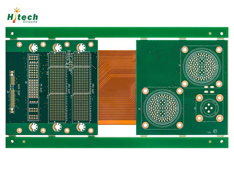
Rigid flex printed circuit boards (PCBs) are manufactured by combining rigid and flexible board technologies. These circuit boards are made up of multiple flexible circuit inner layers. An epoxy pre-preg bonding film is used to attach together these
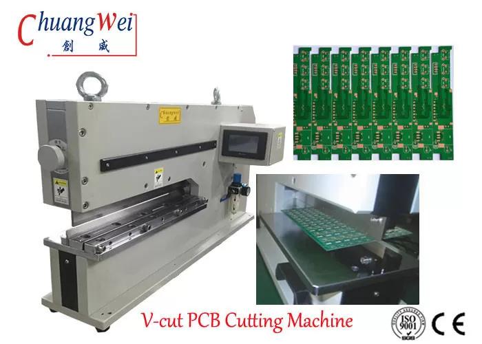
PCB Separator Machine for Metal Board with Linear Blade Advantage: 1. Nice for cutting v cut metal board,Aluminium PCB,LED strip,Copper PCB etc . 2. Separate rigid and thick board fluently . 3. Use pneumatic-driven and electromagnetic valve to oper
Used SMT Equipment | Semiconductor & Solar
Standard Machine features and system description: Ultra-fine pitch and small ball bonding capabilities High frequency transducer operating at 138 kHz Applicable wire size of 0.6mil-2.0mil High speed XY table with linear motor technology High ac
Technical Library | 2023-11-14 19:52:11.0
The continuous drive in the Electronics industry to build new and innovative products has caused competitive design companies to develop assemblies with consolidated PCB designs, decreased physical sizes, and increased performance characteristics. As a result of these new designs, manufacturers of electronics are forced to contend with many challenges. One of the most significant challenges being the processing of thru-hole components on high thermal mass PCBs having the potential to exceed 20 layers in thicknesses and have copper mass contents of over 40oz. High thermal mass PCBs, coupled with the use of mixed technologies, decreased component spacing, and the change from Tin Lead Solder to Lead Free Alloys has lead many manufacturing facilities to purchase advanced soldering equipment to process challenging assemblies with a high degree of repeatability.
Technical Library | 2019-06-20 00:09:49.0
It is well known that during service the layer of Cu6Sn5 intermetallic at the interface between the solder and a Cu substrate grows but the usual concern has been that if this layer gets too thick it will be the brittleness of this intermetallic that will compromise the reliability of the joint, particularly in impact loading. There is another level of concern when the Cu-rich Cu3Sn phase starts to develop at the Cu6Sn5/Cu interface and an imbalance in the diffusion of atomic species, Sn and Cu, across that interface results in the formation at the Cu3Sn/Cu interface of Kirkendall voids, which can also compromise reliability in impact loading. However, when, as is the case in some microelectronics, the copper substrate is thin in relation to the volume of solder in the joint an overriding concern is that all of the Cu will be consumed by reaction with Sn to form these intermetallics.This paper reports an investigation into the kinetics of the growth of the interfacial intermetallic, and the consequent reduction in the thickness of the Cu substrate in solder joints made with three alloys, Sn-3.0Ag-0.5Cu, Sn-0.7Cu-0.05Ni and Sn-1.5Bi-0.7Cu-0.05Ni.

Rigid flex printed circuit boards (PCBs) are manufactured by combining rigid and flexible board technologies. These circuit boards are made up of multiple flexible circuit inner layers. An epoxy pre-preg bonding film is used to attach together these
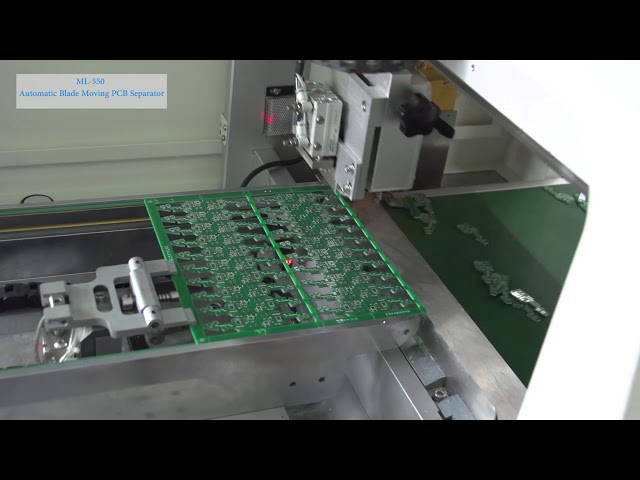
ML-550 Automatic Blade Moving PCB Separator Features ●Suitable for horizontal designed PCB with V-scored groove. ●Automatic feeding and precise positioning to separate PCBA. ●PCB material:FR4.Aluminum,Copper,etc. ●49 sets of PCB data can be stor
ASYMTEK Products | Nordson Electronics Solutions | https://www.nordson.com/-/media/Files/Nordson/efd/Products/Data-Sheets/Thermal-Compound/Nordson_EFD_Thermal_Compound_Selector_Guide.pdf?la=en
. Mechanics of Heat Transfer Choosing the best thermal compound requires some understanding of the mechanics of heat transfer and how the thickness of the thermal compound layer, the bond line