Industry Directory | Consultant / Service Provider / Manufacturer
Designer & Manufacturer of Acoustic Microscopes for Nondestructive Component Inspection.
Our edge-hardened, pre-sharpened knife steel, which we refer to it as �Presharp,� is a high technology, lead-hardened steel that has revolutionized the die-making process. One of Austria�s oldest and most respected steel mills developed a unique proc
Zymet's underfill encapsulants for flip chips are designed to enhance the thermal cycle performance. They incorporate silica filler, used to reduce the encapsulant’s CTE, that are highly engineered in both morphology and particle size distribution to
Electronics Forum | Thu Sep 24 18:57:03 EDT 2009 | davef
From "siliconfareast.com": Basic Die Cracking FA Flow 1) Failure Information/Device and Lot History Review. Understand the customer's description of the failure, i.e., the failure mode, where it was encountered, what conditions the sample was subject
Electronics Forum | Thu Sep 24 09:25:24 EDT 2009 | davef
What do you mean by "substrate?" Is it: * Semiconductor die * BT circuit board interposer Is the BGA package: * Encapsulated * Mounted on a circuit board
Industry News | 2015-06-11 16:02:18.0
MIRTEC, "The Global Leader in Inspection Technology," will exhibit its most recent solutions for System in Package (SiP) inspection and measurement at SEMICON WEST 2015; July 14-16, 2015, at the Moscone Center in San Francisco, CA. Visitors are invited to booth # 2343 for a detailed demonstration of this exciting new technology.
Industry News | 2017-04-24 19:04:48.0
This year, MIRTEC will launch several new inspection machines equipped new cutting-edge technologies. MIRTEC is proud to be promoting these new machines in booth #1J10 at NEPCON China 2017, one of the biggest technical exhibitions of SMT and EMA, from April 25-27 at the Shanghai World EXPO Exhibition & Convention Center. MIRTEC’s new machines have been developed under a concept, ‘Perfect Inspection Solution’. This is an inspection concept involving the combination of 3D, 2D, and side-camera inspection.
Technical Library | 2023-08-16 18:20:44.0
One of our defense customers planned to dispense underfill material for small and large die, using Hysol FP4545FC epoxy encapsulant. This process dissipates stress on solder joints and prevents cracking and fracturing between the bottom of the die and the surface of the substrate.
Technical Library | 2017-06-22 17:11:53.0
C-mode scanning acoustic microscopy (C-SAM) is a non-destructive inspection technique showing the internal features of a specimen by ultrasound. The C-SAM is the preferred method for finding “air gaps” such as delamination, cracks, voids, and porosity. This paper presents evaluations performed on various advanced packages/assemblies especially flip-chip die version of ball grid array/column grid array (BGA/CGA) using C-SAM equipment. For comparison, representative x-ray images of the assemblies were also gathered to show key defect detection features of the two non-destructive techniques.
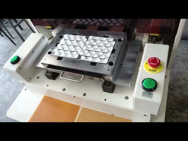
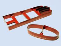
FPC / PCB Punching Dies PCB Depaneler For High Volume Boards Singulation Advantages: 1. Pneumatic, environmental protection 2. High efficiency, suitable for high volume PCBs 3. Security door protection, ensure safe production Features: 1. D
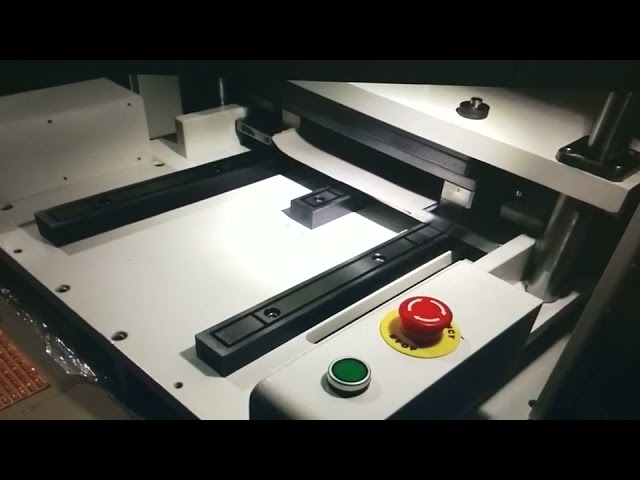
Flexible PCB Board Cutting Machine PCB Punching Machine With Cutomized Die Tooling PCB Punching Machine Features: 1. Depaneling PCB/FPC by means of punching dies, to avoid micro-cracks caused by manual. 2. Die toolings is changeable 3. Easy set
Career Center | , District of Columbia | Engineering,Management,Production,Sales/Marketing
• Strong technical leadership and decision-making skills; strong verbal and written communication skills to provide clear, crisp direction for key issue resolution; and good team skills to facilitate cross-functional cross -site team effectiveness.
| https://www.eptac.com/wp-content/uploads/2013/08/eptac_08_21_13-1.pdf
Heller Industries Inc. | https://hellerindustries.com/wp-content/uploads/2018/07/last-will-of-bga-void.pdf
. An opposing school of thought was that voids act as crack arrestors, which improve solder joint life. The root cause of voids in BGA solder joints is well understood by the electronics industry with a number of papers published on the topic [1, 2, 3]. R


.gif)
winsouce.jpg)