
Specification: Outline size:620*500*820mm (L*W*H) Working Range:320*390*70mm(X*Y*Z) Drive mode:3 axis driver Position accuracy :±0.02mm Control system:PLC + TP Screw Feeding : absorption type Operation method :by Programming Working Speed:
.jpg)
Layer Count: 8L Board Thickness: 1.0mm Panel Dimension:190*86mm/2up Material: S1141 Copper on board surface: 35μm Min Hole Diameter: 0.1mm Min line Width/Space: 8/8mil Surface Finish: ENIG+Selective OSP in BGA area This quick turn PCB is manufacture
Electronics Forum | Wed Jun 23 18:23:32 EDT 1999 | Tom B.
Even though you may find a pad-pad thru-hole spacing, part body size, orientation, and insertion head tooling clearences may be the deciding factor in spacing. 1. Part body diameter will dictate component centroid spacing. ---[][][][
Electronics Forum | Tue Jun 30 18:37:19 EDT 1998 | Earl Moon
| Hi all . | Thanks to Ryan, Brian , Justin and Dave for the timely help earlier. | I would appreciate if somebody could help me in the stated issue: | I am trying to to place one thru hole 20 pin connector along with the SMT components by paste pri
Industry News | 2017-05-11 17:06:16.0
Library Expert Lite automatically builds footprints and 3D STEP models for tens of millions of parts, for free.
Industry News | 2018-10-18 11:18:14.0
Making Readable Silkscreen Layouts for your Printed Circuit Board (PCB) Design

Welcome to this Bob Willis Defect of the Month video on BGA inspection, this series of videos were produced for and featured as part of the NPL/IPC video library and examples are taken from the NPL Defect Database. Over the last couple of years there
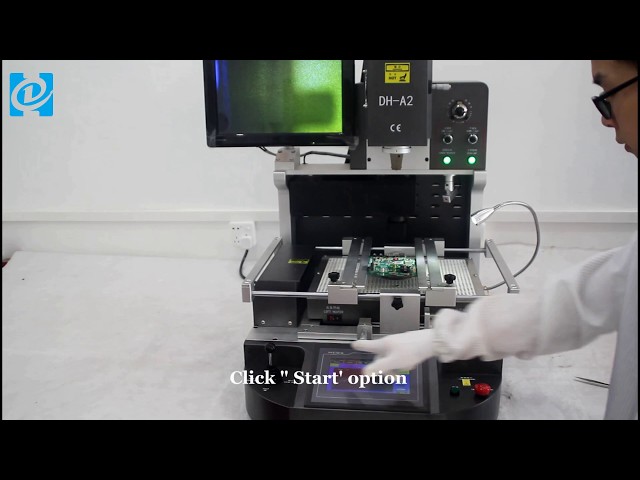
Dinghua Technology-- the leading manufacturer of BGA rework station, Automatic screw locking machine, Automatic soldering station and non-standard equipment. For more details, please just contact John, WhatsApp/Wechat:+86 1576811 4827 , Skype: si
SMT Express, Volume 2, Issue No. 3 - from SMTnet.com Volume 2, Issue No. 3 Thursday, March 16, 2000 Featured Article Return to Front Page Stencil Design for Mixed Technology Through-hole / SMT Placement and Reflow by William E. Coleman, Photo
ORION Industries | http://orionindustries.com/pdfs/SILPADA2000.pdf
. Please contact Inside Sales for additional thickness information. TOLERANCES 0.015 inch tolerances are held on width, length, hole diameters and hole locations
| https://www.eptac.com/soldertip/soldertips-defining-shear-forces-for-surface-mounted-components/
. Based upon best manufacturing and design practices, IPC does have specifications to design circuit pads/land and they use the JEDEC criteria for pad/land size layouts related to individual components


