Electronics Forum | Tue Jul 06 18:16:14 EDT 1999 | Boca
| | Is anyone aware of some guidelines regarding through-hole in SMT pads? One of our designers wants to add through-hole leads in some SMT pads for an inductor. The size of the hole is 0.032 inches and takes-up approximately 25% of the pad area.
Electronics Forum | Tue Jul 06 17:03:46 EDT 1999 | Earl Moon
| Is anyone aware of some guidelines regarding through-hole in SMT pads? One of our designers wants to add through-hole leads in some SMT pads for an inductor. The size of the hole is 0.032 inches and takes-up approximately 25% of the pad area. Th
Industry News | 2016-09-14 17:44:33.0
IPC – Association Connecting Electronics Industries® will present “PCB Troubleshooting” on November 2, 2016 in Raleigh, N.C. in conjunction with regional trade show, PCB Carolina.
Industry News | 2010-09-30 00:35:51.0
The new E revisions of IPC’s popular desk reference manuals, IPC-DRM-PTH, Through-Hole Solder Joint Evaluation Training & Reference Guide and IPC-DRM-SMT, Surface Mount Solder Joint Evaluation Training & Reference Guide have been released.
Technical Library | 2007-06-06 15:25:30.0
Though today's microvias and high aspect plated through holes (PTH's) look nothing like the earliest through holes of 40 years ago, the PTH in its various forms remains the “weak link” and most critical element of printed wiring boards and laminate chip carriers (...) The paper outlines an approach to evaluating PTH reliability and quality that involves characterizing PTH life across a range of temperatures to reveal intricacies not seen by testing at a single delta-T, and certainly difficult to predict by modeling alone.
Technical Library | 2018-09-21 10:12:53.0
Moisture accumulates during storage and industry practice recommends specific levels of baking to avoid delamination. This paper will discuss the use of capacitance measurements to follow the absorption and desorption behaviour of moisture. The PCB design used in this work, focused on the issue of baking out moisture trapped between copper planes. The PCB was designed with different densities of plated through holes and drilled holes in external copper planes, with capacitance sensors located on the inner layers. For trapped volumes between copper planes, the distance between holes proved to be critical in affecting the desorption rate. For fully saturated PCBs, the desorption time at elevated temperatures was observed to be in the order of hundreds of hours. Finite difference diffusion modelling was carried out for moisture desorption behaviour for plated through holes and drilled holes in copper planes. A meshed copper plane was also modelled evaluating its effectiveness for assisting moisture removal and decreasing bake times. Results also showed, that in certain circumstances, regions of the PCB under copper planes initially increase in moisture during baking.
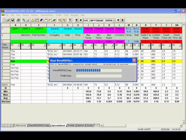
The following video guides the user through a typical data collection process. These steps may vary depending on the process your company uses. Categories: WaveRIDER, WaveRIDER SPC (v5.2x)
Training Courses | | | PCB Assembly Courses
The PCB assembly courses provide knowledge of different processes and equipment used in TH and SMT assembly of printed circuit boards.
SMT Express, Volume 2, Issue No. 3 - from SMTnet.com Volume 2, Issue No. 3 Thursday, March 16, 2000 Featured Article Return to Front Page Stencil Design for Mixed Technology Through-hole / SMT Placement and Reflow by William E. Coleman, Photo
Heller Industries Inc. | https://hellerindustries.com/wicking-defetcs/
× Re-printed in partnership with ITM Wicking Defects Defect: wicking A Wicking Defect is the flow of solder either up the lead of the component or along traces and possibly under insulation and through via holes
| https://www.eptac.com/webinars/plated-through-hole-fill-understanding-the-process-and-assembly-requirements/
Plated Through Hole Fill: Understanding the Process and Assembly Requirements - EPTAC - Train. Work Smarter. Succeed Looking for solder training standards, manuals, kits, and more


