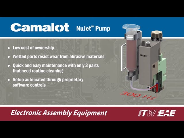
New Equipment | Rework & Repair Services
In order to maintain the highest level of quality in electronics, most manufacturers will employ some form of process control methodology to identify faulty conditions or potential quality variances. The feedback provided by such a system must natur
SMT Flexible Pick and Place Machine Flex-6 If you could not find any similar items you want, you may send some photos to us. because our catalog and website haven't included all of our products. Pick and place machine, SMT pick and place mach
Electronics Forum | Thu Jun 11 09:28:57 EDT 2020 | pcbkathay
Dear Luciano, We are PCB manufactured based in China,we can produce the PCB as your requirements as soon as we can, please send the files to my email 284816044@qq.com looking foward to your email.
Electronics Forum | Thu Jun 11 02:32:54 EDT 2020 | beanzheng0
Hi, Luciano This is James from http://www.nextpcb.com We can do your order we have 2 manufacturers over 2500000sq. The 4 layer PCB boards on sale now. Please send your inquiry to support@nextpcb.com Or you can contact me on WhatsApp:+8613243830029 S
Used SMT Equipment | Chipshooters / Chip Mounters
Hello and thank you for your interest in our (2) FUJI CP43 and (1) FUJI IP3 Machines For Sale. These(3) machines are being sold together in package. The equipment just came out of a Military Defense Electronics Manufacturing Company. It is in good co
.png)
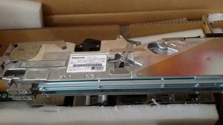
Used SMT Equipment | Assembly Accessories
Panasonic's BM231 modular high speed multi-functional placement machine boasts any volume, any mix capability by placing a wide array of components from 0402 (01005) microchips to BGA's, CSP's and connectors. Outstanding productivity is a
Industry News | 2003-03-25 08:31:07.0
On completion of the transaction, Flairis will become a wholly-owned subsidiary of Beyonics and its shares will be delisted from Sesdaq.
Industry News | 2003-03-11 08:45:00.0
CAMtastic DXP is the latest version of Altium's complete CAM verification and editing system that bridges the gap between PCB design and manufacturing and facilitates communication between board designers, fabrication engineers, and their clients.

Parts & Supplies | Pick and Place/Feeders
Detailed Product Description KXFW1KS9A00 , 72mm feeder with sensor CM/NPM Feeder For CM602 machine We provide CM602 Feeders,all kinds of feeders are in the warehouse,expecially 8mm , 12/16mm ,stick feeder....etc. , this feeder part number is KXFW
Parts & Supplies | Pick and Place/Feeders
Detailed Product Description KXFW1KS9A00 , 72mm feeder with sensor CM/NPM Feeder For CM602 machine We provide CM602 Feeders,all kinds of feeders are in the warehouse,expecially 8mm , 12/16mm ,stick feeder....etc. , this feeder part number is KXFW
Technical Library | 2020-04-01 14:24:56.0
It happens much too often; manufacturing engineers are brought into a NEW product design phase at the very end of a design and are asked to provide input that should have been provided much earlier. One needs to understand how the circuit board design and quality of the manufacturing process not only effects assembly yield and product reliability, but how it could also affect the results of any testing that is done to circuit packs during prototyping. It is important that any circuit pack (including prototypes) that will be used in reliability, performance and functional testing be designed with the proper features and assembled with a manufacturing process that has been developed to produce a high-quality assembly. If not, the results of any testing might not represent the actual characteristics of the design and provide miss-guidance to future changes.
Technical Library | 2020-08-27 01:22:45.0
Initially adopted internal specifications for acceptance of printed circuit boards (PCBs) used for wire bonding was that there were no nodules or scratches allowed on the wirebond pads when inspected under 20X magnification. The nodules and scratches were not defined by measurable dimensions and were considered to be unacceptable if there was any sign of a visual blemish on wire-bondable features. Analysis of the yield at a PCB manufacturer monitored monthly for over two years indicated that the target yield could not be achieved, and the main reasons for yield loss were due to nodules and scratches on the wirebonding pads. The PCB manufacturer attempted to eliminate nodules and scratches. First, a light-scrubbing step was added after electroless copper plating to remove any co-deposited fine particles that acted as a seed for nodules at the time of copper plating. Then, the electrolytic copper plating tank was emptied, fully cleaned, and filtered to eliminate the possibility of co-deposited particles in the electroplating process. Both actions greatly reduced the density of the nodules but did not fully eliminate them. Even though there was only one nodule on any wire-bonding pad, the board was still considered a reject. To reduce scratches on wirebonding pads, the PCB manufacturer utilized foam trays after routing the boards so that they did not make direct contact with other boards. This action significantly reduced the scratches on wire-bonding pads, even though some isolated scratches still appeared from time to time, which caused the boards to be rejected. Even with these significant improvements, the target yield remained unachievable. Another approach was then taken to consider if wire bonding could be successfully performed over nodules and scratches and if there was a dimensional threshold where wire bonding could be successful. A gold ball bonding process called either stand-off-stitch bonding (SSB) or ball-stitch-on-ball bonding (BSOB) was used to determine the effects of nodules and scratches on wire bonds. The dimension of nodules, including height, and the size of scratches, including width, were measured before wire bonding. Wire bonding was then performed directly on various sizes of nodules and scratches on the bonding pad, and the evaluation of wire bonds was conducted using wire pull tests before and after reliability testing. Based on the results of the wire-bonding evaluation, the internal specification for nodules and scratches for wirebondable PCBs was modified to allow nodules and scratches with a certain height and a width limitation compared to initially adopted internal specifications of no nodules and no scratches. Such an approach resulted in improved yield at the PCB manufacturer.
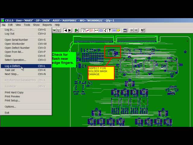
www.unisoft-cim.com/cells.html - CELLS WORKFLOW is affordable, simple to setup & use yet powerful product & job tracking software for fast New Product Introduction (NPI). The CELLS WORKFLOW software provides total traceability in manufacturing floor
Training Courses | | | PCB Inspection Courses
The PCB inspection courses focus on improving PCB yield and reliability through validation and detection of defects on electronics assemblies.
Training Courses | ON DEMAND | | IPC-6012 Trainer (CIT)
The Certified IPC-6012 Trainer (CIT) courses recognize individuals as qualified trainers in the area of design, fabrication and inspection of rigid printed boards and prepare them to deliver Certified IPC-6012 Specialist (CIS) training.
Events Calendar | Thu Jun 01 00:00:00 EDT 2023 - Thu Jun 01 00:00:00 EDT 2023 | Aguascalientes, Mexico
Aguascalientes Expo and Tech Forum
Events Calendar | Wed May 31 00:00:00 EDT 2023 - Wed May 31 00:00:00 EDT 2023 | Holtsville, New York USA
Long Island Chapter Meeting: Fine Feature Paste Printing, Stencil Design and Solder Technology
Career Center | Manhattan, Kansas USA | Production
Ultra Electronics, ICE is a leader in small aircraft aerospace systems and components. ICE secured its first contract in the aircraft industry in 1975 by designing and manufacturing a state-of-the-art deicer timer for Cessna Aircraft Company. ICE c
Career Center | Rocklin, California USA | Production
General Overview of Position With this new position Parallax aims to improve our USA manufacturing throughput in a time when most companies normally only send work offshore. This raises the standard for requiring efficient use of our Pick and Place
SMT Express Submission Guidelines SMTnet provides electronics manufacturing professionals with the latest product, process, and industry information that helps them to do their jobs. Our over-riding criteria is interest and relevance
Surface Mount Technology Association (SMTA) | https://www.smta.org/education/presentations/presentations.cfm
. Three surface finishes including OSP, ImAg, and ENIG are considered. The test vehicle consists of 15mm and 6mm Ball Grid Array (BGA) components. The assembled test boards were isothermally aged at 125oC for 12 months, which are then thermally cycled between -40oC to
| https://www.smtfactory.com/SMT-PCB-Coating-line-with-of-New-Designed-and-and-High-Efficiency-pd47161624.html
SMT PCB Coating line with of New Designed and and High Efficiency from China manufacturer - I.C.T SMT Machine English Türk dili Tiếng Việt 한국어 日本語 Italiano Deutsch