New Equipment | Rework & Repair Equipment
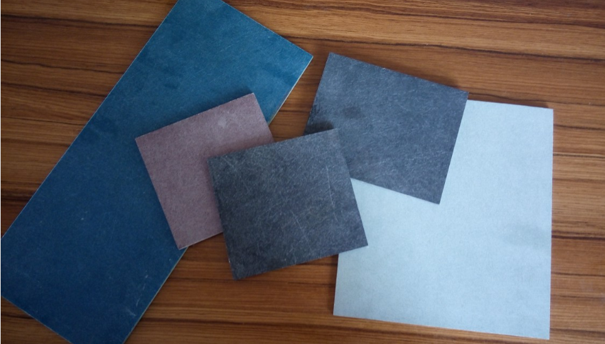
This unique rework stenciling system is very simple to use. Adhesive Backed Stencil Thickness: 004in (.10mm), .005in (.13mm) and .006in (.15mm) Minimum Aperture Size: .002in (.05mm) Stencil Material: Plastic film with release liner. The adhesive bac
New Equipment | Board Handling - Pallets,Carriers,Fixtures
Durastone wave pallet material with good price Overview: 1, Durostone materials are reinforced glass fibre composites. 2, It have been proved to be suitable for all processes during PCB assembly such as SMT reflow and wave soldering processes.
Electronics Forum | Sun Apr 03 00:34:56 EST 2005 | Andrew
Can anyone advise the best aperture opening and stencil thickness for Nexlev connector?We are seeing high reject for open solder.
Electronics Forum | Tue Jun 28 14:06:08 EDT 2011 | dmiller
If you have room, and the aperture size will allow for it, try a 5 mil overall stencil thickness with a 1 mil step-up in the area of the BGA connector.
Industry News | 2003-03-21 08:12:24.0
Tecan reckons it is consistently producing what may be regarded as the most efficient stencils in the world today.
Industry News | 2018-10-18 10:13:08.0
The Application of the Pin-in-Paste Reflow Process
Technical Library | 2018-06-13 11:42:00.0
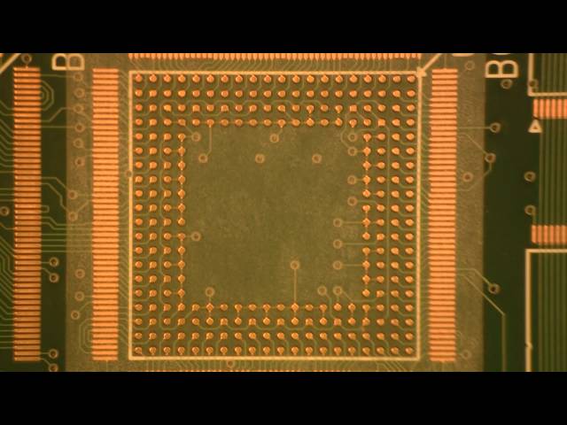
The art of screen printing solder paste for the surface mount community has been discussed and presented for several decades. However, the impending introduction of passive Metric 0201 devices has reopened the need to re-evaluate the printing process and the influence of stencil architecture. The impact of introducing apertures with architectural dimensions’ sub 150um whilst accommodating the requirements of the standard suite of surface mount connectors, passives and integrated circuits will require a greater knowledge of the solder paste printing process.The dilemma of including the next generation of surface mount devices into this new heterogeneous environment will create area ratio challenges that fall below todays 0.5 threshold. Within this paper the issues of printing challenging area ratio and their associated aspect ratio will be investigated. The findings will be considered against the next generation of surface mount devices.
Technical Library | 2023-07-25 16:50:02.0
Some of the new handheld communication devices offer real challenges to the paste printing process. Normally, there are very small devices like 01005 chip components as well as 0.3 mm pitch uBGA along with other devices that require higher deposits of solder paste. Surface mount connectors or RF shields with coplanarity issues fall into this category. Aperture sizes for the small devices require a stencil thickness in the 50 to 75 um (2-3 mils) range for effective paste transfer whereas the RF shield and SMT connector would like at least 150 um (6 mils) paste height. Spacing is too small to use normal step stencils. This paper will explore a different type of step stencil for this application; a "Two-Print Stencil Process" step stencil. Here is a brief description of a "Two-Print Stencil Process". A 50 to 75 um (2-3 mils) stencil is used to print solder paste for the 01005, 0.3 mm pitch uBGA and other fine pitch components. While this paste is still wet a second in-line stencil printer is used to print all other components using a second thicker stencil. This second stencil has relief pockets on the contact side of the stencil any paste was printed with the first stencil. Design guidelines for minimum keep-out distances between the relief step, the fine pitch apertures, and the RF Shields apertures as well relief pocket height clearance of the paste printed by the first print stencil will be provided.
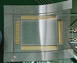
Demonstration of BGA rework via stencil printing. BEST's StikNPeel stencil is an adhesive backed stencil which allows users to stick the stencil in to place and simply peel it off the PCB with a temporary adhesive system. This leaves consistent print
Career Center | Bangalore, India | Engineering,Maintenance,Production,Technical Support
SMT Stencil designing & Knowledge of full SMT process software known CAD/CAM -circuit CAM Pro 7.3,GC Power station, GCCAM Edit,Auto CAD, Fault finding of Electronic Boards & Servicing electronic machines.
SMTnet Express, June 14, 2018, Subscribers: 31,125, Companies: 10,958, Users: 24,820 Unlocking The Mystery of Aperture Architecture for Fine Line Printing Clive Ashmore; ASM Assembly Systems The art of screen printing solder paste for the surface
40731 | https://www.smta.org/smtai/SMTAI-2019-Technical-Program.pdf?v=200609010628
Surface Mount Technology Association (SMTA)
GPD Global | https://www.gpd-global.com/co_website/pdf/doc/Dispense-System-Service-Guide-22290008G.pdf
items to the service panel: – Printer cord (to serial or parallel port on rear panel) – Ethernet connections – SMEMA cables - if only the incoming connector is used, connect it to the downstream (left) port and terminate the upstream (right) port


