Industry Directory | Consultant / Service Provider / Manufacturer
SemiPack Services is an Electronic Manufacturing Support Service to the semiconductor industry. We specialize in providing support services to high-mix low-volume (HMLV) customers
Industry Directory | Manufacturer
Near Shore Assembly for Microelectronics Circuitry

New Equipment | Board Handling - Storage
Solder paste printing range (1) SMT technology of resistance, capacitance, inductance, diode, triode and other chip components production and processing: 01005, 0201, 04020603, 0805, 1206 and other specifications and sizes; (2) , IC: support SOP, T
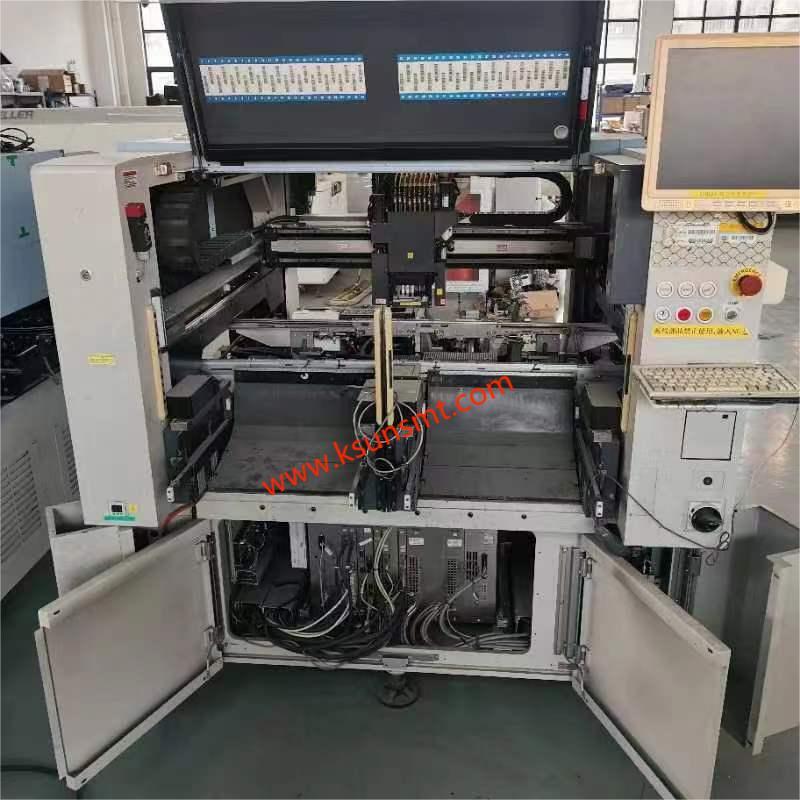
YAMAHA YG100R HIGH SPEED PICK AND PLACE MACHINE Model YG100RA(FNC TYPE )/YG100RB(SF TYPE) Object substrate L50×W50mm ~L510×W460mm Mounting efficiency 24000CPH/CHIP (
Electronics Forum | Fri Mar 19 10:02:44 EDT 2010 | karlo
There is a wide range of BGA underfills to satisfy specific needs. Some are designed for those who place a premium on high speed, high volume processing, shock or drop test perforamnce, and ease of reworkability. Others are designed for those who p
Electronics Forum | Tue Oct 15 20:33:43 EDT 2002 | davef
First, this is a very interesting question. Second, there is no specification. Third, companies develop guidelines for rework based on their expectations for their product reliability. Things to consider are: * Motorola allows no product shipments

Used SMT Equipment | Screen Printers
DEK Horizon 03i automatic stencil printer Specification : DEK Horizon 03i High Precision Automatic Solder Paste Printer designed for high precision steel mesh printing or stencil printing in SMT industry. Printing PCB size: 50x50mm to 508x510mm;

Used SMT Equipment | SMT Equipment
Product name: KE - 3010 A high-speed chip mounter Product number: KE – 3010A Detailed product introduction Characteristic: Constantly improve the KE series products. So as to realize the high speed high quality electric production line of flexib
Industry News | 2014-06-22 19:12:37.0
MIRTEC, “The Global Leader in Inspection Technology,” will exhibit in Booth #5444-1 at SEMICON West 2014, scheduled to take place July 8-10 at the Moscone Center in San Francisco, CA.
Industry News | 2003-04-15 08:57:18.0
First Implementation of the Package Platform Delivers 50-percent Cost, 60-percent Height, and 75-percent Area Reductions over Conventional RF Module Technologies

Parts & Supplies | SMT Equipment
SMT Pick And Place Equipment Parts JUKI 730 740 750 760 1700 1710 IMG-P IMAGE BOARD E86107210A0 Specifications: Brand Name JUKI IMG-P IMAGE BOARD Part number E86107210A0 Model IMG-P Ensure Test in machine confirmation Guarantee 3 month u
Parts & Supplies | SMT Equipment
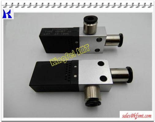
SMT SPARE PARTS JUKI 750 760 EJECTOR E3066700000 PISCO VBH07-46 JUKI Nozzle Specifications: Brand Name JUKI EJECTOR Part Number E3066700000 Model Number VBH07-46 Ensure Tested buy juki Guarantee 1 month usage for machine JUKI 750 760 Sel
Technical Library | 2023-01-17 17:22:28.0
The impact of voiding on the solder joint integrity of ball grid arrays (BGAs)/chip scale packages (CSPs) can be a topic of lengthy and energetic discussion. Detailed industry investigations have shown that voids have little effect on solder joint integrity unless they fall into specific location/geometry configurations. These investigations have focused on thermal cycle testing at 0°C-100°C, which is typically used to evaluate commercial electronic products. This paper documents an investigation to determine the impact of voids in BGA and CSP components using thermal cycle testing (-55°C to +125°C) in accordance with the IPC- 9701 specification for tin/lead solder alloys. This temperature range is more typical of military and other high performance product use environments. A proposed BGA void requirement revision for the IPC-JSTD-001 specification will be extracted from the results analysis.
Technical Library | 2019-10-21 09:58:50.0
An ACI Technologies customer inquired regarding printed circuit board(PCB) failures that were becoming increasingly prevalent after the SMT (surface mount technology) manufacturing process. The failures were detected by electrical testing, but were undetermined as to the location and specific devices causing the failures. The failures were suspected to be caused predominately in the BGA (ball grid array) devices located on specific sites on this 16 layer construction. Information that was provided on the nature of the failures (i.e., opens or shorts) included high resistance shorts that were occurring in those specified areas. The surface finish was a eutectic HASL (hot air solder leveling) and the solder paste used was a water soluble Sn/Pb(tin/lead).

Precision PCB Services, Inc. to Exhibit at the SMTA’s Tampa Bay Expo & Tech Forum, which will take place on October 5, 2021 at Embassy Suites by Hilton Tampa Airport Westshore. 555 N Westshore Blvd., Tampa Bay, Florida. Pre

Precision PCB Services, Inc. to Exhibit at the SMTA’s Space Coast Expo & Tech Forum, which will take place on October 7, Melbourne Auditorium, 625 E. Hibiscus Blvd., Melbourne, Florida Precision PCB Services, Inc. will be providi
Training Courses | | | PCB Inspection Courses
The PCB inspection courses focus on improving PCB yield and reliability through validation and detection of defects on electronics assemblies.
Training Courses | | | PCB Rework and Hand Soldering Courses
The PCB rework and hand soldering courses courses cover techniques of rework and repair of PCBs, BGAs and other electronics assemblies, and teach fundamentals of soldering of electronics assemblies.
Events Calendar | Mon Mar 18 00:00:00 EDT 2019 - Mon Mar 18 00:00:00 EDT 2019 | ,
Webinar: Stencil Design for Solder Paste, In Process Inspection & Process Defects
Events Calendar | Tue Feb 19 00:00:00 EST 2019 - Tue Feb 19 00:00:00 EST 2019 | ,
Webinar: BGA Reballing - Theory and Hands On
Career Center | South Windsor, Connecticut USA | Engineering,Technical Support
Posting JK-NVPE Process Engineer(PCB Assembly and support)- Our client, located in northern Connecticut, seeks a process engineer capable of providing engineering support in the development and/or improvement of current or new technologies and proces
Career Center | Rochester, New York USA | Engineering
Job Description: Implements and analyzes manufacturing engineering plans and projects. Designs, develops and transfers manufacturing and engineering tools, strategies and systems. Develops manufacturing strategies for specific products and processes
Career Center | , California | Quality Control
Tammy T Vo P.O. Box 2213 (714) 254-5073 E-mail: nhutamvo@yahoo.com Position of Interest Senior Quality Inspector Aerospace Manufacturing. / Electronic PCBA/Advanced coating technologies Profile of Qualifications 12 years of experience wo
Career Center | Delhi, India | Maintenance,Production,Sales/Marketing,Technical Support
7 Years of experiance in SMT line
SMTnet Express, January 5, 2014, Subscribers: 23,708, Members: Companies: 14,158 , Users: 37,476 The Last Will And Testament of the BGA Void Dave Hillman, Dave Adams, Tim Pearson, Brad Williams, Brittany Petrick, Ross Wilcoxon - Rockwell Collins
Head-in-Pillow BGA Defects Head-in-Pillow BGA Defects. Head-in-pillow (HiP), also known as ball-and-socket, is a solder joint defect where the solder paste deposit wets the pad, but does not fully wet the ball. This results in a solder joint
PCB Libraries, Inc. | https://www.pcblibraries.com/forum/RSS_bga-footprint_topic2430.xml
PCB Libraries Forum : BGA Footprint PCB Libraries Forum : BGA Footprint This is an XML content feed of; PCB Libraries Forum : Questions & Answers : BGA Footprint BGA Footprint
Heller Industries Inc. | https://hellerindustries.com/wp-content/uploads/2018/07/last-will-of-bga-void.pdf
. This paper documents an investigation to determine the impact of voids in BGA and CSP components using thermal cycle testing (-55°C to +125°C) in accordance with the IPC- 9701 specification for tin/lead solder alloys


