New Equipment | Cleaning Equipment
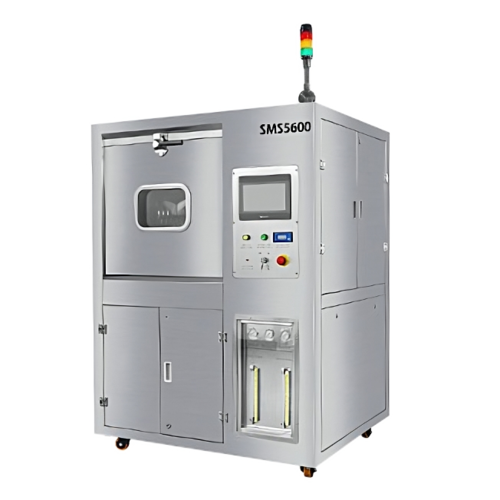
Fully automatic PCBA cleaning machine-SMS-5600 1. Comprehensive cleaning, which can thoroughly clean the residual rosin flux, water-soluble flux, no-clean flux, solder paste and other organic and inorganic pollutants on the surface of PCB after sol
New Equipment | Selective Soldering
I.C.T-SS550 | Full-auto Online Selective Wave Soldering Machine Overview Selective wave soldering is a special form of wave soldering invented to meet the development requirements of through-hole components soldering. It is mainly suitable fo
Electronics Forum | Mon Aug 24 04:46:54 EDT 2009 | joannetjy
Hi Radek, Thanks for your reply. I use this flux with manual soldering process for the product. Is this flux suitable for manual soldering? or it is only for wave soldering? I have sent the board for analysis, and the report shown that the white res
Electronics Forum | Sun Aug 23 22:13:45 EDT 2009 | joannetjy
Hi All, Recently, I need to deal with a customer complaint that specify the PCBA white residue (flux residue from ecofree 303) may be the reason why the board intermittent. Anyone have such experience with this flux? Anyone can tell me is this flux
Used SMT Equipment | In-Circuit Testers
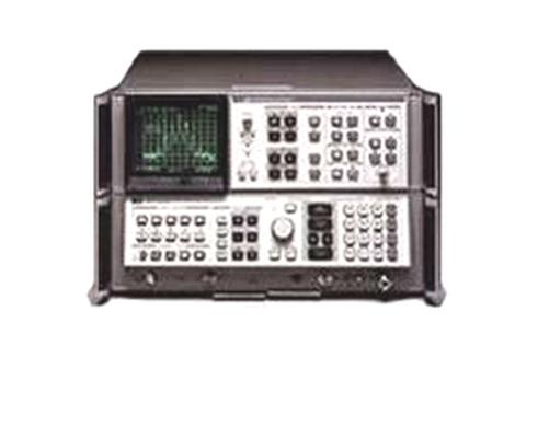
Agilent-Keysight 8568B-001 Spectrum Analyzer, 75 Ohm BNC Input, 100 Hz to 1500 MHz A high-performance, 100 Hz to 1.5 GHz spectrum analyzer for bench and ATE use. The exceptional frequency stability of the HP 8568B permits measurements with a 10
Industry News | 2011-01-22 00:27:29.0
Design, assembly, soldering, repair, rework, inspection, and materials choice are all variables to be juggled as electronics manufacturers worldwide work with new component types, high speed signals and lead-free technology. To assist them in making the best choices for producing reliable electronics, IPC — Association Connecting Electronics Industries® is holding the IPC Conference on Quality, Reliability and Acceptability for Electronics Manufacturing in Budapest, Hungary, on 22–24 February 2011.
Industry News | 2014-10-06 17:27:56.0
Industry-leading associations IPC and SMTA jointly announce the High-Reliability Cleaning and Conformal Coating Conference scheduled to take place November 18-20, 2014 at the Chicago Marriott in Schaumburg, Illinois.
Technical Library | 2019-06-03 15:32:40.0
ACI Technologies was pleased to assist a customer by conducting elemental analysis on several assemblies displaying severe corrosion. Several board assemblies had failed in the field and exhibited areas of corrosion in close proximity to onboard components. The most common source of corrosion on electronic assemblies is residual flux. Fluxes are specific chemistries applied during the soldering process which improve the wetting of the solder to both the pad and component when forming the solder joint. They can be highly reactive chemicals that, if left on the assemblies, can lead to corrosion, electrical degradation, and decreased reliability. In the presence of moisture and electrical bias, flux residue can enable dendritic growth as a result of electrochemical migration (ECM).
Technical Library | 2021-09-02 08:17:07.0
We are a professional manufacturer of PCB depaneling machines, which is workable for all boards, including flex and regid boards, v-scored boards and routed boards. Laser pcb depaneling is non-contact way without mechanical stress,this solution is good for modern precision PCB depaneling. It has below advantages: 1. No dust The production environment of the circuit board industry is carried out in the dust-free workshop. The traditional pcb depaneling equipment, such as blade moving type machine, will inevitably produce residues and micro powder, which will pollute the 10000 and 1000 class dust-free workshops and affect the conductivity of products. The UV laser PCB cutting machine is a vaporization processing process, which will not produce dust and is conducive to the conductivity of the product. 2. High cutting precision The processing gap of high-precision traditional processing equipment can not reach the gap width of less than 100 microns, which will cause certain damage to the lines on the edge or PCBA circuit board containing components. The focus spot of the laser cutting machine is small, and the ultraviolet cold processing mode has little thermal impact on the edge of the circuit board. The cutting position accuracy is less than 50 microns, and the cutting size accuracy is less than 30 microns, which will not affect the edge of the circuit board, and the precision is high. 3. No stress Traditional processing methods generally have V-grooves, which will cause certain damage to the board in the manufacturing process. The UV laser PCB cutting machine can directly cut the bare board without making V-grooves. In addition, the traditional processing methods directly use tools to act on the circuit board, especially the stamping method has a great impact on the circuit board, which is easy to cause board deformation. The laser cutting machine is a non-contact processing mode, which acts on the surface of the material through the high-energy beam, which will not cause the influence of stress and the deformation and damage of the circuit board. 4. For special-shaped cutting, it is easy to automate The UV laser PCB cutting machine can cut for any shape without replacing any props and fixtures, and without steel mesh. The same equipment can meet special-shaped and straight-line cutting, which is easy to realize assembly line automatic production and high flexibility. It is easy to improve production efficiency and save production process and production cycle. In particular, it can quickly and efficiently meet the needs of rapid proofing, directly import the drawing, and then locate the cutting. 5. High compatibility The UV laser PCB cutting machine can process the materials around the circuit board, such as PCB, FPC, covering film, pet, reinforcing board, IC, ultra-thin metal cutting, etc. it has strong practicability, is compatible with the processing of a variety of materials, is easy to operate, can be imported into the drawing, does not need to adjust any mechanical parts, and is easy to operate and maintain. 6. Good cutting edge effect The cutting edge is smooth and neat without burr. It can be processed and formed directly according to the size of the drawing, which is conducive to improving the yield of the product. It can be directly installed into the subsequent process without further processing. For more details about UV laser depaneling, please feel free to contact us. www.pcbdepanelingrouter.com
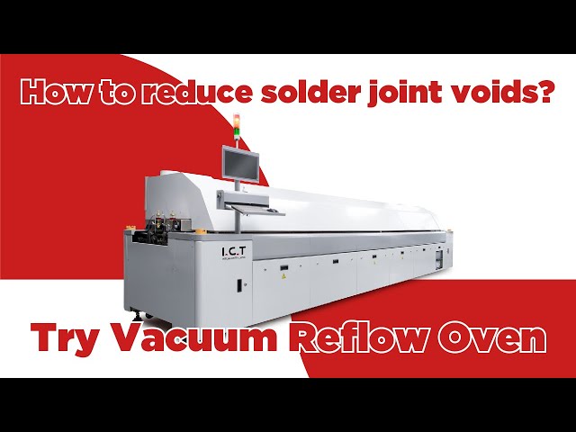
· What is the difference between SMT vacuum reflow soldering machine and ordinary reflow soldering machine? · What problems can be solved by smt vacuum reflow soldering machine? · What is the basic principle of vacuum reflow machine? · Ho
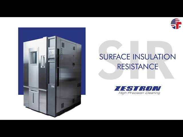
ZESTRON proudly offers SIR testing at our Manassas, VA location. SIR is a quantitative test method used to characterize the PCB manufacturing process residues and their impact on reliability. ZESTRON’s SIR testing capability is offered to clients who
Training Courses | | | PCB Rework and Hand Soldering Courses
The PCB rework and hand soldering courses courses cover techniques of rework and repair of PCBs, BGAs and other electronics assemblies, and teach fundamentals of soldering of electronics assemblies.
Training Courses | ONLINE | | PCB Assembly Courses
The PCB assembly courses provide knowledge of different processes and equipment used in TH and SMT assembly of printed circuit boards.
Events Calendar | Mon May 10 00:00:00 EDT 2021 - Mon May 10 00:00:00 EDT 2021 | ,
Europe Chapter Webinar: Manual Cleaning of Printed Board Assemblies – Step by Step Guide
Events Calendar | Wed Mar 18 00:00:00 EDT 2020 - Wed Mar 18 00:00:00 EDT 2020 | College Park, Maryland USA
CALCE Reliability Science Symposium - Spring 2020
Article Return to Front Page No-Residue Technolo
SMTnet Express, July 28, 2016, Subscribers: 25,879, Companies: 14,883, Users: 40,795 Duo-Solvent Cleaning Process Development for Removing Flux Residue from Class 3 Hardware Mike Bixenman, DBA - Kyzen Corporation | Ryan Hulse, PHD - Honeywell
| http://etasmt.com/cc?ID=te_news_bulletin,23574&url=_print
>> News Circuit Board Voids & PCB Delamination Circuit Board Voids Circuit Board Voids are cavities or air pockets inside the solder joint formed by gases that are released during reflow or by flux residues that fail to escape
| https://www.smtfactory.com/PCBA-Cleaning-Machine-PCB-Defluxing-For-Best-Coating-and-Bonding-Effect-id43566387.html
. PCB must be thoroughly cleaned of production residues as well as dirt to ensure reliable further processing and trouble-free performance


