New Equipment | Education/Training
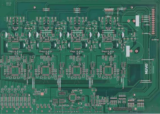
This specification covers qualification and performance of rigid PCBs including with or without plated-through holes, single-sided, double-sided, multilayer with or without blind/buried vias and metal core boards. It addresses final finish and surfac
New Equipment | Industrial Automation
new and original!!GE IC200GBI001 new and original!!GE IC200GBI001 Contact :Sandy Lin Email: unity@mvme.cn Mob/Whatsapp :+ 86 18020776786 Tel : +86 592 5165503 Skype: onlywnn_1 Wechat : mooreplc website : www.sa
Electronics Forum | Fri Nov 03 07:28:27 EST 2006 | davef
Via filling methods are: * Tenting * Plugging * Capping * Flooding Tented Via. A via covered with dry film soldermask; the via is not filled. When tenting from both sides there may be issues with trapped air that expands during mass soldering. Plug
Electronics Forum | Wed Sep 18 14:12:40 EDT 2013 | pjchonis
Hello Bachman. SAC305 is the most common lead-free solder alloy, not only for wave soldering but also selective. Most of our selective customers (especially automotive) are using SAC305. What is more important than the alloy to consider is the flux
Industry News | 2003-03-11 08:45:00.0
CAMtastic DXP is the latest version of Altium's complete CAM verification and editing system that bridges the gap between PCB design and manufacturing and facilitates communication between board designers, fabrication engineers, and their clients.
Industry News | 2010-04-10 02:09:54.0
If a picture is worth a thousand words, the new H revision of IPC-A-600, Acceptability of Printed Boards, is a priceless work of art for fabricators and assemblers, particularly inspectors and product developers. IPC — Association Connecting Electronics Industries® announces the new releases of IPC-A-600H and its companion document the C revision of IPC-6012, Qualification and Performance Specification for Rigid Printed Boards.
Technical Library | 2019-07-17 17:56:34.0
The increased demand for electronic devices in recent years has led to an extensive research in the field to meet the requirements of the industry. Electrolytic copper has been an important technology in the fabrication of PCBs and semiconductors. Aqueous sulfuric acid baths are explored for filling or building up with copper structures like blind micro vias (BMV), trenches, through holes (TH), and pillar bumps. As circuit miniaturization continues, developing a process that simultaneously fills vias and plates TH with various sizes and aspect ratios, while minimizing the surface copper thickness is critical. Filling BMV and plating TH at the same time, presents great difficulties for the PCB manufactures. The conventional copper plating processes that provide good via fill and leveling of the deposit tend to worsen the throwing power (TP) of the electroplating bath. TP is defined as the ratio of the deposit copper thickness in the center of the through hole to its thickness at the surface. In this paper an optimization of recently developed innovative, one step acid copper plating technology for filling vias with a minimal surface thickness and plating through holes is presented.
Technical Library | 2020-03-12 13:10:35.0
The electronics industry is further progressing in terms of smaller, faster, smarter and more efficient electronic devices. This continuous evolving environment caused the development on various electrolytic copper processes for different applications over the past several decades. (...) This paper describes the reasons for development and a roadmap of dimensions for copper filled through holes, microvias and other copper plated structures on PCBs.
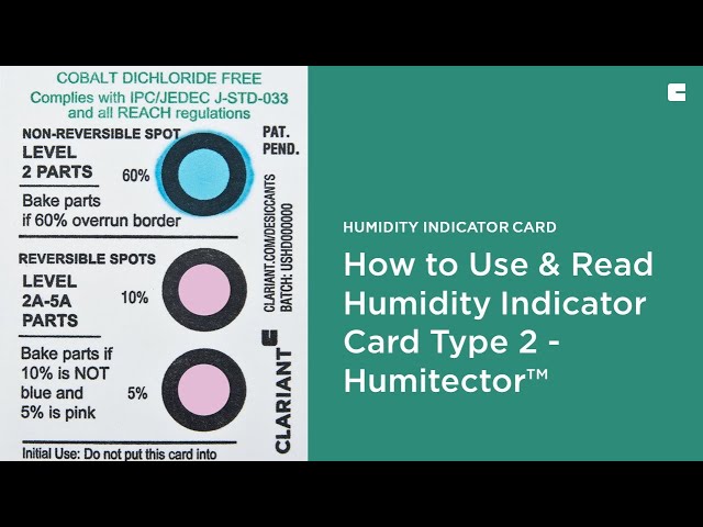
A Sustainable Alternative - Humitector cards are halogen-free and cobalt dichloride free. Visit https://www.clariant.com/solutions/products/2017/10/31/00/12/humitector-type-2-nonreversible-humidity-indicator-card?utm_source=CLRYouTube&utm_medium=Vi
This video describes the IPC A-600 training and certification program. The IPC A-600 specification is a set of acceptability specifications for printed circuit boards. These standards determine the acceptance and reject criteria for printed wiring bo
Training Courses | ON DEMAND | | IPC-600 Trainer (CIT)
The Certified IPC-600 Trainer (CIT) courses recognize individuals as qualified trainers in the area of quality assurance of bare printed circuit boards and prepare them to deliver Certified IPC-600 (CIS) training.
Training Courses | ON DEMAND | | IPC-6012 Trainer (CIT)
The Certified IPC-6012 Trainer (CIT) courses recognize individuals as qualified trainers in the area of design, fabrication and inspection of rigid printed boards and prepare them to deliver Certified IPC-6012 Specialist (CIS) training.
Events Calendar | Tue Dec 04 00:00:00 EST 2018 - Tue Dec 04 00:00:00 EST 2018 | ,
Qualification and Reliability of Microvias
SMTnet Express, June 27, 2019, Subscribers: 32,092, Companies: 10,819, Users: 24,882 Advanced Cu Electroplating Process for Any Layer Via Fill Applications with Thin Surface Copper Credits: MacDermid Inc. Copper-filled micro-vias are a key
SMTnet Express, May 12, 2022, Subscribers: 25,588, Companies: 11,569, Users: 27,213 Electronics Manufacturing Technical Articles Filling of Microvias and Through Holes by Electrolytic Copper Plating –Current Status and Future
Surface Mount Technology Association (SMTA) | https://www.smta.org/education/presentations/presentations.cfm
Cost of Gold, Copper, Palladium, Silver, tin etc Protective coatings and effects of soldering operations Solderability reflow wetting patterns Solderability tests: Dip and inspect, wetting balance, rotary dip test Simple
Imagineering, Inc. | https://www.pcbnet.com/blog/hdi-pcb-advantages-and-applications/
(High Density Interconnect) technology is increasingly becoming the solution for smaller, more durable, and more efficient PCBs. HDI technology allows for lighter, smaller products that do more faster than ever before by leveraging blind and buried vias that can be staggered, stacked, and integrated with microvias


