Industry Directory | Manufacturer
R&D, production and sales of chemicals, equipment and related materials used in the production of PCB
Industry Directory | Manufacturer
Qualitetch utilse photo etching, wire EDM, laser cutting, metal forming, machining to offer the "Total Metal Component Solution" to customers requiring thin gauge metal components in most metals.
New Equipment | Rework & Repair Equipment
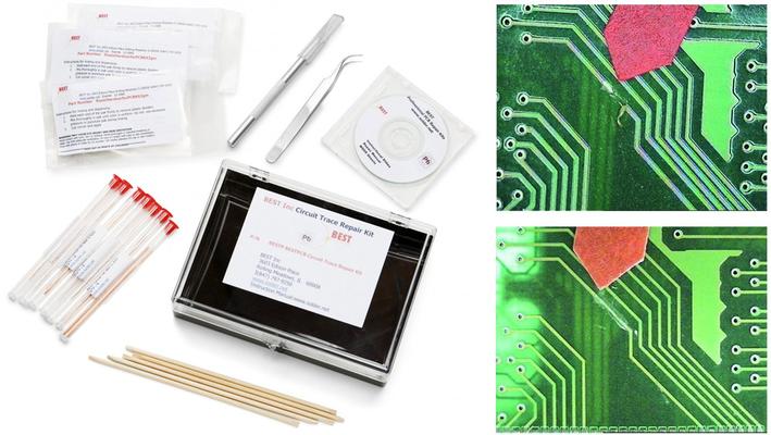
The BEST PCB circuit trace repair kit gives you the tools you need for fast modification and repair of PCB circuit traces. Our online PCB repair training videos, our master instructors along with these materials allows you to meet the original PCB qu
.jpg)
Item Description Stamping contact spring famliy Material : Spring steel,Stainless steel,Cooper,Beryllium copper, Brass,phosphor copper ,etc... Shield type :More shapes ,more thinckness Dimension: As your drawing Tolerance: per drawing ,If you ha
Electronics Forum | Wed Oct 16 01:28:45 EDT 2002 | redmary
during the failure analysis, how to etch the tin,nickle,and copper?
Electronics Forum | Thu Oct 17 23:25:53 EDT 2002 | redmary
We generally etch the copper back slightly using a 50/50 mix of 3% Hydrogen Peroxide and laboratory grade Ammonium Hydroxide. Swab for about 5 seconds, then rinse. and etch the tin in the solder to further delineate the intermetallic layer that shou
Industry News | 2003-02-07 09:13:12.0
The Sessions Covered Current and Emerging Technologies
Industry News | 2003-03-12 08:28:44.0
CAM350 Release 8 is aimed at allowing engineering and manufacturing groups to detect and fix potential PCB fabrication problems earlier in the process.
Technical Library | 2020-11-29 22:06:45.0
Plastic laminates are increasingly used as interposers within chip packaging applications. As a component within the package, the laminate is subjected to package moisture sensitivity testing. The moisture requirements of chip packaging laminates are related to ambient moisture absorption and thermal cycling. Printed wiring board (PWB) laminates, however, are gauged on properties relating to wet processes such as resist developing, copper etching, and pumice scrubbing. Consequently, printed wiring board moisture absorption test methods differ from chip packaging test conditions.
Technical Library | 2017-11-22 12:38:51.0
The use of copper foils laminated to polyimide (PI) as flexible printed circuit board precursor is a standard practice in the PCB industry. We have previously described[1] an approach to very thin copper laminates of coating uniform layers of nano copper inks and converting them into conductive foils via photonic sintering with a multibulb conveyor system, which is consistent with roll-to-roll manufacturing. The copper thickness of these foils can be augmented by electroplating. Very thin copper layers enable etching fine lines in the flexible circuit. These films must adhere tenaciously to the polyimide substrate.In this paper, we investigate the factors which improve and inhibit adhesion. It was found that the ink composition, photonic sintering conditions, substrate pretreatment, and the inclusion of layers (metal and organic) intermediate between the copper and the polyimide are important.

PCB pad circuit repair using epoxy. Using multiple angles including overhead and from both right and left angles the BEST instructor staff demonstrates plainly how to repair a PCB pad using the epoxy method. This method is per IPC 7721 4.4.1. http://
PCB pad circuit repair using epoxy. Using multiple angles including overhead and from both right and left angles the BEST instructor staff demonstrates plainly how to repair a PCB pad using the epoxy method. This method is per IPC 7721 4.4.1. http://
Career Center | Erode, Tamilnadu India | Engineering
Professional Summary 3+ years of experience in the PCB CAM engineering Exposure to FRONTLINE GENESIS 2000 Having exposure in UCAM Exposure to Create, Array & Panelize it for manufacturability Experienced in Creating impedance cou
Career Center | Shen Zhen, China | Management,Sales/Marketing
Working in GLORYPCB for 10 years.knowing electronic supply chain very well. especially for PCB PCBA assembly and other Electronic Manufacturing Service.Glorypcb is a professional electronic manufacturer located in Shenzhen with three facilities.offe
SMTnet Express, November 22, 2017, Subscribers: 31,034, Companies: 10,792, Users: 24,082 Factors Affecting the Adhesion of Thin Film Copper on Polyimide David Ciufo, Hsin-Yi Tsai and Michael J. Carmody; Intrinsiq Materials Inc. The use of copper
Imagineering, Inc. | https://www.pcbnet.com/blog/how-pcbs-are-made/
. Copper Cladding Copper cladding is then added to the substrate through a process called copper lamination or copper plating. Cladding involves applying a thin layer of copper to the surface of the substrate, which creates a conductive pathway for traces. III. Photoengraving (Etching
ASYMTEK Products | Nordson Electronics Solutions | https://www.nordson.com/en/divisions/march/process/anisotropic-and-isotropic-etch?con=t
: Anisotropic and Isotropic Etch Controlled Chemical Plasma Etching for Advanced Technology Applications Nordson MARCH CS-1701 Anisotropic RIE Plasma System Nordson MARCH Please see the RIE Series for


