Industry Directory | Consultant / Service Provider / Manufacturer
Providing production and prototype, SEC offers advanced technologies like LED thermal management, heavy copper, PTFE for RFMW, open and internal cavities and blind and buried vias that are certified to a diverse set of industries.
Industry Directory | Consultant / Service Provider / Manufacturer
Manufacturer of highly miniaturized and high reliability PCBs. Swiss Quality substrates for demanding applications such as implants and medical devices. HDI flex, rigid-flex and rigid PCBs in small to medium volumes.
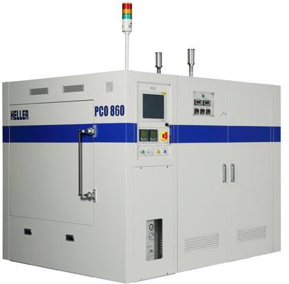
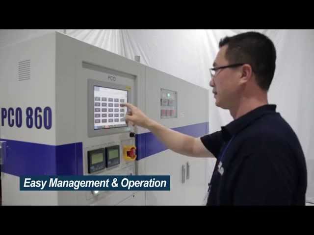
New Equipment | Curing Equipment
A Pressure Cure Oven (PCO), or Autoclave, is used to minimize voiding and increase adhesion strength for bonding processes typically used in die attach and underfill applications. PCO pressurizes air into a rigid vessel and heats & cools with
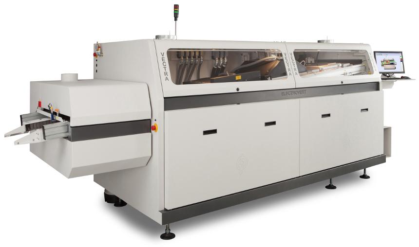
New Equipment | Wave Soldering
The Ideal Wave Soldering System for Low-to-Medium Volume Lead-free Pproduction. The award-winning ELECTROVERT VectraES wave soldering system features exceptional system-wide accessibility, an advanced control system and innovative sub-system technol
Electronics Forum | Fri Oct 08 09:43:27 EDT 2004 | davef
First, don't get too excited about the thermal capabilities of conductive epoxy. An epoxy like DuPont CB-100 increases the amount of heat conducted through the barrel, but many over estimate what it can do. Calculations show for a 0.020" drilled
Electronics Forum | Fri Oct 08 07:38:48 EDT 2004 | Paddy
Hello, I am wondering if anybody has process experiance of designs which use the above. I understand that the filled via is an excellent thermal cnductor, which is great from a design point of view, but how do these solder through the reflow ovens
Industry News | 2011-02-04 01:47:14.0
GPD Global will highlight its Positive Cavity Displacement (PCD) Dispensing at the upcoming SMTA Dallas Expo & Tech Forum, scheduled to take place Tuesday, March 1, 2011 at the Richardson Civic Center in Richardson, TX.
Industry News | 2011-02-07 15:23:56.0
GPD Global will highlight its Positive Cavity Displacement (PCD) Dispensing at the upcoming SMTA Houston Expo & Tech Forum, scheduled to take place Thursday, March 3, 2011 at the Stafford Centre in Stafford, TX.
Technical Library | 2014-11-13 19:23:50.0
With increasing power loss of electrical components, thermal performance of an assembled device becomes one of the most important quality factors in electronic packaging. Due to the rapid advances in semiconductor technology, particularly in the regime of high-power components, the temperature dependence of the long-term reliability is a critical parameter and has to be considered with highest possible care during the design phase (...) The aim of this paper is to give a short overview about standard thermal solutions like thick copper, thermal vias, plugged vias or metal core based PCBs. Furthermore, attention will be turned on the development of copper filled thermal vias in thin board constructions...
Technical Library | 2021-05-26 00:53:26.0
This paper describes a copper electroplating enabling technology for filling microvias. Driven by the need for faster, smaller and higher performance communication and electronic devices, build-up technology incorporating microvias has emerged as a viable multilayer printed circuit manufacturing technology. Increased wiring density, reduced line widths, smaller through-holes and microvias are all attributes of these High Density Interconnect (HDI) packages. Filling the microvias with conductive material allows the use of stacked vias and via in pad designs thereby facilitating additional packaging density. Other potential design attributes include thermal management enhancement and benefits for high frequency circuitry. Electrodeposited copper can be utilized for filling microvias and provides potential advantages over alternative via plugging techniques. The features, development, scale up and results of direct current (DC) and periodic pulse reverse (PPR) acid copper via filling processes, including chemistry and equipment, are described.
General curing, die attach curing, underfill curing, film & tape bonding, wafer laminating.
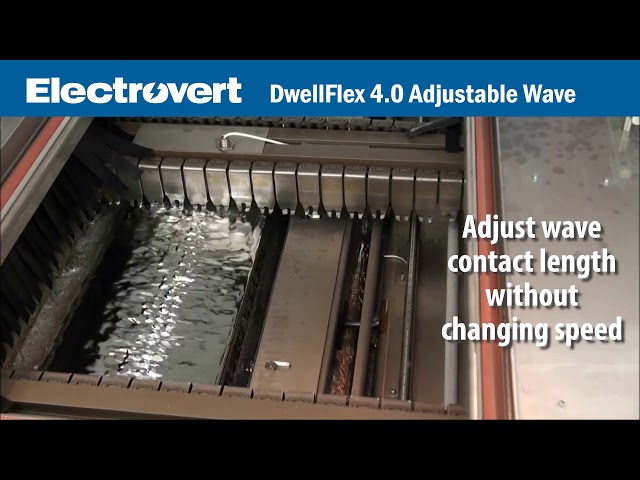
Electrovert's DwellFlex 4.0 is the first solder nozzle designed specifically with Industry 4.0 automation in mind. The patent pending design enables the length of the wave to be adjusted on-the-fly as variable board types are run through the wave.
Training Courses | | | IPC-6012 Specialist (CIS)
The Certified IPC-6012 Specialist (CIS) training covers design, fabrication and inspection of rigid printed boards.
Training Courses | | | Other Courses
Other courses related to electronics manufacturing and assembly
Events Calendar | Mon Apr 23 00:00:00 EDT 2018 - Thu Apr 26 00:00:00 EDT 2018 | Shanghai, China
SMTA China East Conference 2018
Career Center | Erode, Tamilnadu India | Engineering
Professional Summary 3+ years of experience in the PCB CAM engineering Exposure to FRONTLINE GENESIS 2000 Having exposure in UCAM Exposure to Create, Array & Panelize it for manufacturability Experienced in Creating impedance cou
Career Center | Alta Loma, California | Engineering,Quality Control,Research and Development
Rigid and Flexible Printed Circuits Plating and Metal Finishing Operations Six Sigma Work Instruction Documentation Process Development Equipment Selection and Specification New Facility Startup Air, Water and Hazardous Waste Environmental Reporting
SMTnet Express, May 12, 2022, Subscribers: 25,588, Companies: 11,569, Users: 27,213 Electronics Manufacturing Technical Articles Filling of Microvias and Through Holes by Electrolytic Copper Plating –Current Status and Future
SMTnet Express, June 27, 2019, Subscribers: 32,092, Companies: 10,819, Users: 24,882 Advanced Cu Electroplating Process for Any Layer Via Fill Applications with Thin Surface Copper Credits: MacDermid Inc. Copper-filled micro-vias are a key
| https://www.eptac.com/faqs/ask-helena-leo/ask/soldering-thick-pcbs-with-3-oz-copper
Soldering Thick PCB's With 3 oz Copper - EPTAC - Train. Work Smarter. Succeed Looking for solder training standards, manuals, kits, and more
Imagineering, Inc. | https://www.pcbnet.com/blog/the-importance-of-thermal-management-in-pcb-manufacturing/
. Thermal loads are most easily dissipated by the use of copper layering, vias placed under power components, the use of cold walls, thermal padding, and component spacing


