Industry Directory | Manufacturer
Multilay,HDI,thick copper and Aluminium boards'supplier
Industry Directory | Manufacturer
US manufacturer of metallized ceramic substrates & packages; specializing in PCTF (plated copper over thick film) & low cost AgENIG (silver with electroless nickel and immersion gold plating).
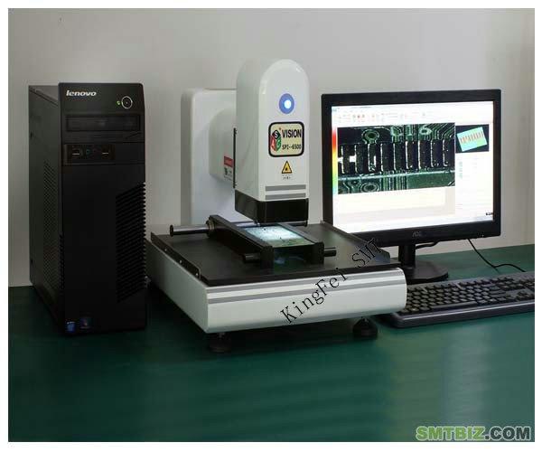
New Equipment | Assembly Services
Detailed introduction of 3D spi-6500 solder paste thickness gauge Product function 1. Friendly programming interface 2. Multiple measurement methods 3. The scanning distance is adjustable 4. 3D simulation function of image 5. Independent
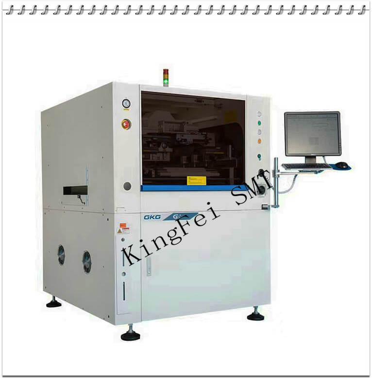
New Equipment | Assembly Services
G9 + automatic vision printing machine is a new product for SMT high-end application field, which can perfectly meet the process requirements of 03015, 0.25pich and other fine spacing, high precision and high speed. Introduction to standard function
Electronics Forum | Mon Nov 14 12:10:05 EST 2005 | davef
Ceramic capacitors larger then EIA size 1812 are known to be very susceptible to thermal shock damage due to their large ceramic mass.
Electronics Forum | Mon Nov 07 16:34:55 EST 2005 | CW
If I am putting chip capacitors on a .063 FR4 board, what size package should we stay away from to avoid cracking? If I use 2 mil copper on the outside layers of a PCB, am I limited to what pitch of parts I can use? Specifically, will using 0603
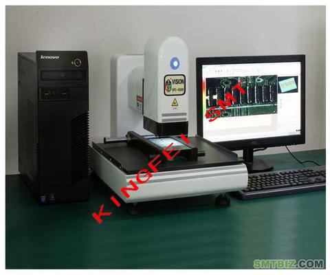
Used SMT Equipment | Pick and Place/Feeders
Product Details of 3D SPI-6500 Thick Paste Measurement Instrument Product Functions 1, friendly programming interface 2, a variety of measurement methods 3, scan spacing adjustable 4, image 3D simulation function 5, independent 3D dynamic obser
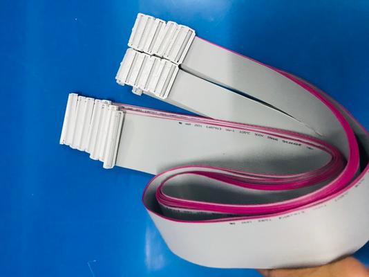
Used SMT Equipment | Hand Assembly
electrical wire 6 8 12 14 16 20 24 44 50 64 pin 2.54 mm pitch idc connectors flat ribbon cable PRODUCT DESCRIPTION ★Rated temperature:80ºC ★Rated voltage:300V ★According to:UL Subject758,UL62,C22.2 ★Solid or stranded,tinned or bare copper
Industry News | 2003-06-24 08:14:51.0
R/flex� 3850 laminate is produced in a range of copper and LCP thicknesses, just as the single-clad laminate, and is available in standard panel formats.
Industry News | 2015-02-15 17:55:40.0
The best technical conference paper of IPC APEX EXPO 2015 has been selected. Voted on through a ballot process by members of IPC’s Technical Program Committee, the paper authors will receive their awards during the opening keynote session on Tuesday, February 24.
Parts & Supplies | Assembly Accessories
PC12P Inventory Material: Copper Clad FR4, Single Sided, 2 oz. Series: - Size Dimension: 18.00" x 12.00" (457.4mm x 304.8mm) Board Thickness: 0.062" (1.57mm) 1/16" Proto Board Type: Copper Clad, Positive Sensitized PC12P-E RFQ
_1.jpg)
Parts & Supplies | Pick and Place/Feeders
FUJI PM0BAD0 RETAINER, SPRING Other Fuji parts: H4569A BEARING, MINIATURE Belt Drive Tooth Bearing PM25490 SPACER belt drive tooth copper gasket AA76203 GEAR belt drive tooth PJ00162 GEAR waste belt gear (thick) PM03602 PIN ↑ fixed PIN K5357M
Technical Library | 2020-07-22 19:39:05.0
The PWB industry needs to complete reliability testing in order to define the minimum copper wrap plating thickness requirement for confirming the reliability of PTH structures. Predicting reliability must ensure that the failure mechanism is demonstrated as a wear-out failure mode because a plating wrap failure is unpredictable. The purpose of this study was to quantify the effects of various copper wrap plating thicknesses through IST testing followed by micro sectioning to determine the failure mechanism and identify the minimum copper wrap thickness required for a reliable PWB. Minimum copper wrap plating thickness has become an even a bigger concern since designers started designing HDI products with buried vias, microvias and through filled vias all in one design. PWBs go through multiple plating cycles requiring planarization after each plating cycle to keep the surface copper to a manageable thickness for etching. The companies started a project to study the relationship between Copper wrap plating thickness and via reliability. The project had two phases. This paper will present findings from both Phase 1 and Phase 2.
Technical Library | 2019-07-17 17:56:34.0
The increased demand for electronic devices in recent years has led to an extensive research in the field to meet the requirements of the industry. Electrolytic copper has been an important technology in the fabrication of PCBs and semiconductors. Aqueous sulfuric acid baths are explored for filling or building up with copper structures like blind micro vias (BMV), trenches, through holes (TH), and pillar bumps. As circuit miniaturization continues, developing a process that simultaneously fills vias and plates TH with various sizes and aspect ratios, while minimizing the surface copper thickness is critical. Filling BMV and plating TH at the same time, presents great difficulties for the PCB manufactures. The conventional copper plating processes that provide good via fill and leveling of the deposit tend to worsen the throwing power (TP) of the electroplating bath. TP is defined as the ratio of the deposit copper thickness in the center of the through hole to its thickness at the surface. In this paper an optimization of recently developed innovative, one step acid copper plating technology for filling vias with a minimal surface thickness and plating through holes is presented.
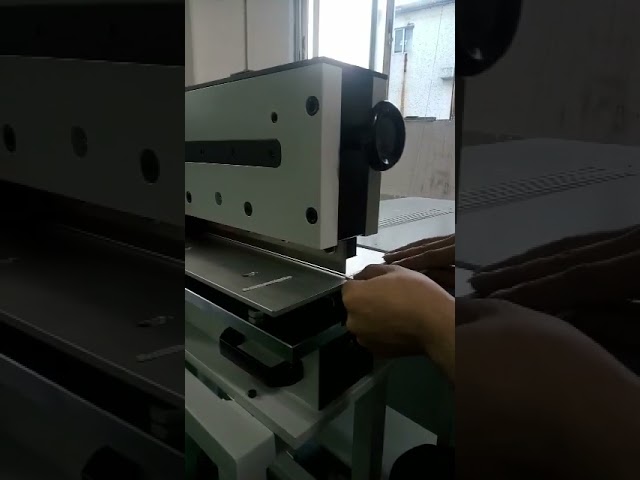
Guillotine type V-cut PCB Cutting Machine Product Description 1. For internal strength generates during separation, Minimize it to value under 180uE ,to avoid solder crack or component damage 2. Able to separate edge of V-slot, minimum distance to
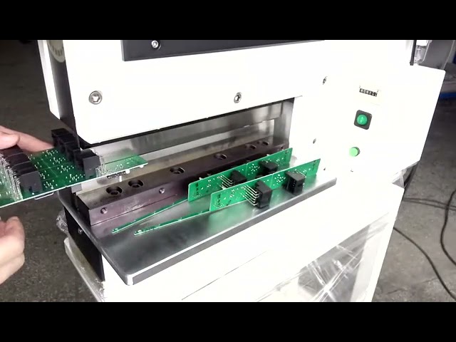
Metal Board V-cut PCB Depaneling Machine Guillotine PCB Cutter Features: 1. Less stress ,high cutting quality 2. Suitable for cutting all kinds of PCB material, even for Aluminum and copper material PCBs. 3. Security:the cutting opening is 2mm t
Training Courses | | | IPC-6012 Specialist (CIS)
The Certified IPC-6012 Specialist (CIS) training covers design, fabrication and inspection of rigid printed boards.
Training Courses | | | IPC-600 Specialist (CIS)
The Certified IPC-600 Specialist (CIS) training targets quality assurance and acceptance of bare printed circuit boards.
Events Calendar | Wed Mar 18 00:00:00 EDT 2020 - Wed Mar 18 00:00:00 EDT 2020 | College Park, Maryland USA
CALCE Reliability Science Symposium - Spring 2020
Career Center | Shen Zhen, China | Management,Sales/Marketing
Working in GLORYPCB for 10 years.knowing electronic supply chain very well. especially for PCB PCBA assembly and other Electronic Manufacturing Service.Glorypcb is a professional electronic manufacturer located in Shenzhen with three facilities.offe
Career Center | Erode, Tamilnadu India | Engineering
Professional Summary 3+ years of experience in the PCB CAM engineering Exposure to FRONTLINE GENESIS 2000 Having exposure in UCAM Exposure to Create, Array & Panelize it for manufacturability Experienced in Creating impedance cou
SMTnet Express, November 22, 2017, Subscribers: 31,034, Companies: 10,792, Users: 24,082 Factors Affecting the Adhesion of Thin Film Copper on Polyimide David Ciufo, Hsin-Yi Tsai and Michael J. Carmody; Intrinsiq Materials Inc. The use of copper
Imagineering, Inc. | https://www.pcbnet.com/capabilities/assembly/tolerances/
Clad, Other Copper Thickness: < 2 oz. Call for other options Learn About Imagineering Have questions? Contact Us Ready to get started
| http://etasmt.com/cc?ID=te_news_industry,24563&url=_print
. When you need to optimize the reflow profile, you need to analyze the board parameters such as board thickness, copper thickness, and components as well as be familiar with your reflow oven’s capability. Keywords


