Industry Directory | Manufacturer
professional manufacturer of pcb
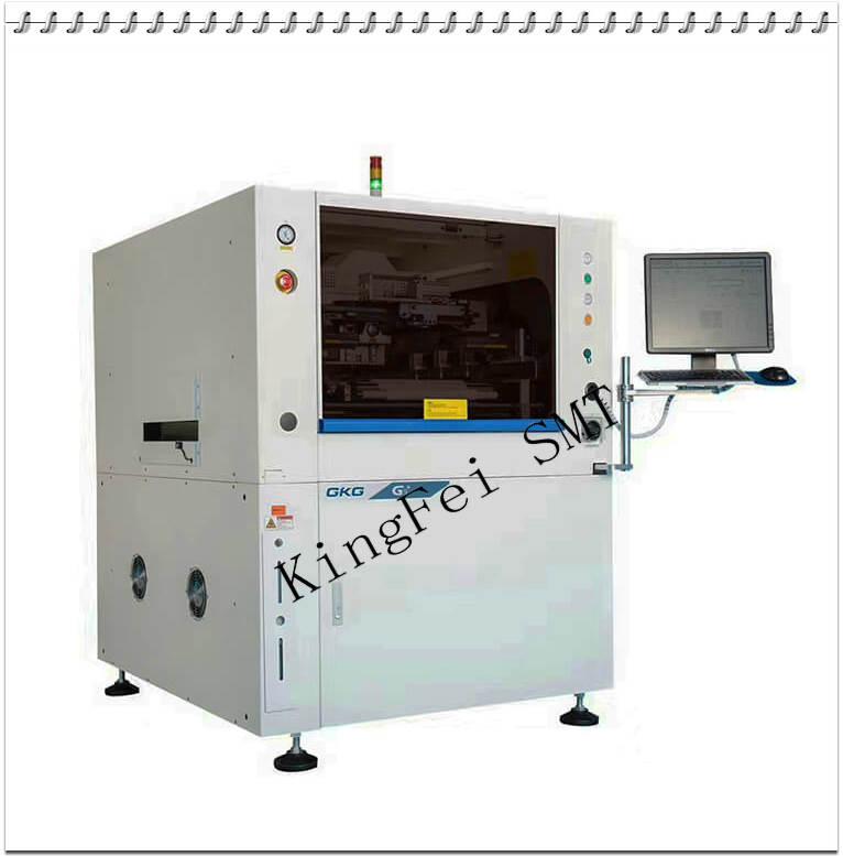
New Equipment | Assembly Services
G9 + automatic vision printing machine is a new product for SMT high-end application field, which can perfectly meet the process requirements of 03015, 0.25pich and other fine spacing, high precision and high speed. Introduction to standard function
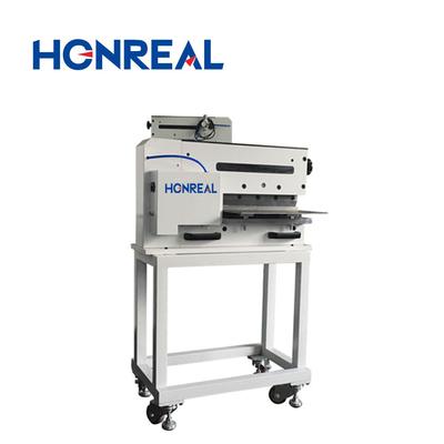
Guillotine type V-cut PCB Cutting Machine Product Description 1. For internal strength generates during separation, Minimize it to value under 180uE ,to avoid solder crack or component damage 2. Able to separate edge of V-slot, minimum distance to
Electronics Forum | Tue Nov 08 05:00:23 EST 2005 | rlackey
Hi CW, Regarding orientation, yes, your diagram is right - see the following link for confirmation. http://search.murata.co.jp/Ceramy/image/img/A18X/C2EB3C.PDF Regarding information on bending strength you want to talk to your local Murata office
Electronics Forum | Thu Oct 02 11:04:48 EDT 2003 | russ
Out of curiousity, Isn't soldermask only used as a solder processing aid and to cover the copper? Russ
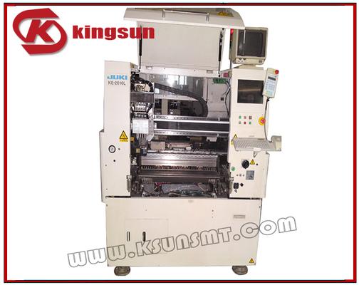
Used SMT Equipment | SMT Equipment
Product name: KE - 2060 l JUKI chip mounter Product number: KE - 2060 l JUKI2060 chip mounter parameters: Mounting head: 3 Material stand: 80 Mount speed: 0.25 SEC/CHIP (3 head at the same time put in the attached SMT) Mounting speed:+ / - 0.
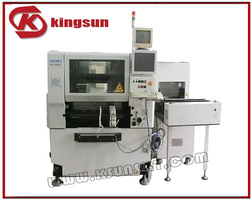
Used SMT Equipment | SMT Equipment
Product name: KE - 2010 l JUKI chip mounter Product number: KE - 2010 l Products in detail Substrate size: Min: 50 mmx30mm Max: 330 mmx250mm Substrate thickness: Min: 0.4 mm Max: 4 mm Element size: 0402 ~ 20 mm square element or 26.5 X11mm Mo
Industry News | 2023-10-16 12:50:01.0
MIRTEC announces the release of their All-New ART Hybrid 3D AOI System at Productronica 2023. The World's leading trade fair for the electronics manufacturing industry will take place Nov. 14-17, 2023, at the Trade Fair Center Messe München, Germany. All are welcome to MIRTEC's Booth #461 in Hall A2 for a detailed demonstration of what will undoubtedly be recognized as the World's Most Technologically Advanced 3D AOI System!
Industry News | 2003-06-10 08:16:44.0
The following text describes the application of NWA Quality Analyst to quality control in the assembly of electronic components.

Parts & Supplies | SPI / Solder Paste Inspection
Quick programming, friendly programming interface Multiple measurement methods True one-button measurement Eight-way motion button, one-click focus Adjustable scanning pitch Solder paste 3D simulation function Powerful SPC function MARK
Technical Library | 2020-07-22 19:39:05.0
The PWB industry needs to complete reliability testing in order to define the minimum copper wrap plating thickness requirement for confirming the reliability of PTH structures. Predicting reliability must ensure that the failure mechanism is demonstrated as a wear-out failure mode because a plating wrap failure is unpredictable. The purpose of this study was to quantify the effects of various copper wrap plating thicknesses through IST testing followed by micro sectioning to determine the failure mechanism and identify the minimum copper wrap thickness required for a reliable PWB. Minimum copper wrap plating thickness has become an even a bigger concern since designers started designing HDI products with buried vias, microvias and through filled vias all in one design. PWBs go through multiple plating cycles requiring planarization after each plating cycle to keep the surface copper to a manageable thickness for etching. The companies started a project to study the relationship between Copper wrap plating thickness and via reliability. The project had two phases. This paper will present findings from both Phase 1 and Phase 2.
Technical Library | 2019-07-17 17:56:34.0
The increased demand for electronic devices in recent years has led to an extensive research in the field to meet the requirements of the industry. Electrolytic copper has been an important technology in the fabrication of PCBs and semiconductors. Aqueous sulfuric acid baths are explored for filling or building up with copper structures like blind micro vias (BMV), trenches, through holes (TH), and pillar bumps. As circuit miniaturization continues, developing a process that simultaneously fills vias and plates TH with various sizes and aspect ratios, while minimizing the surface copper thickness is critical. Filling BMV and plating TH at the same time, presents great difficulties for the PCB manufactures. The conventional copper plating processes that provide good via fill and leveling of the deposit tend to worsen the throwing power (TP) of the electroplating bath. TP is defined as the ratio of the deposit copper thickness in the center of the through hole to its thickness at the surface. In this paper an optimization of recently developed innovative, one step acid copper plating technology for filling vias with a minimal surface thickness and plating through holes is presented.
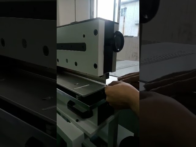
Guillotine type V-cut PCB Cutting Machine Product Description 1. For internal strength generates during separation, Minimize it to value under 180uE ,to avoid solder crack or component damage 2. Able to separate edge of V-slot, minimum distance to
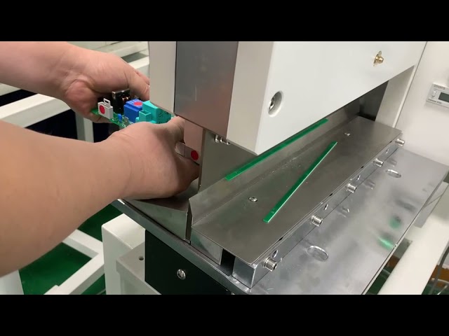
600mm Penumatic V-groove PCB Cutter Linear Blades PCB Separator Penumatic V-groove PCB Cutter Description: In order to improve the output of printed circuit board (PCB) manufacturing and the linear speed of surface mount (SMT), the printed circ
Training Courses | | | IPC-600 Specialist (CIS)
The Certified IPC-600 Specialist (CIS) training targets quality assurance and acceptance of bare printed circuit boards.
Training Courses | | | PCB Design Courses
The PCB design courses teach students the process, techniques and tools needed to design layout of printed circuit boards.
Events Calendar | Wed Mar 18 00:00:00 EDT 2020 - Wed Mar 18 00:00:00 EDT 2020 | College Park, Maryland USA
CALCE Reliability Science Symposium - Spring 2020
Career Center | Erode, Tamilnadu India | Engineering
Professional Summary 3+ years of experience in the PCB CAM engineering Exposure to FRONTLINE GENESIS 2000 Having exposure in UCAM Exposure to Create, Array & Panelize it for manufacturability Experienced in Creating impedance cou
Career Center | Shen Zhen, China | Management,Sales/Marketing
Working in GLORYPCB for 10 years.knowing electronic supply chain very well. especially for PCB PCBA assembly and other Electronic Manufacturing Service.Glorypcb is a professional electronic manufacturer located in Shenzhen with three facilities.offe
ATTENDANT WET CHEMICAL PROCESSES) Hole wall preparatio
ASCEN Technology | https://www.ascen.ltd/Blog/machine/PCB_depaneling_machine/844.html
> PCB depaneling machine > fully automatic PCB depaneling trimming processing separator machine : PCB depaneling machine, :2021-08-01 PCB depaneling often happen right after SMT processing or after soldering,or after in-circuit test in the assembly
Imagineering, Inc. | https://www.pcbnet.com/quote/board-quote-usa/?cpn=2
. $1,500 Free Special Introductory Offer (For Bare Boards Only) If you are placing orders through our website, after placing your first order, call us at 847-806-0003


