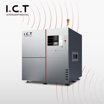
Inline 3D PCB Automated X-ray Inspection System - Advanced Quality Assurance Solution ❙ Introduce of SMT PCBA X-ray Machine Explore our Inline 3D PCB Automated X-ray Inspection System, a cutting-edge solution for advanced quality assurance in PCB
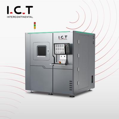
Off-line 3D SMT X-ray Inspection Machine - High-precision Quality Control ❙ Introduce of SMT PCBA X-ray Machine Looking for an off-line 3D SMT X-ray inspection machine? Our high-precision 3D SMT X-ray machine ensures top-notch quality control for
Electronics Forum | Mon Jan 12 21:31:26 EST 2015 | warwolf
The closer your inspection the more defects you will find, the more rework you do the possible cost you will add and the potential increase of damage you could do to your products if rework is not up to a machine copyable standard. "Is there any in
Electronics Forum | Wed Jun 15 12:23:46 EDT 2011 | gregcr
Hi All, I'm gathering information on what is available for BGA inspection. I have worked with a few x-ray systems, but would like any input on CT Scan systems. thanks
Industry News | 2012-01-23 00:02:12.0
MIRTEC, “The Global Leader in Inspection Technology”, will premier its complete line of 3D AOI, SPI, X-ray and LED inspection systems at the IPC APEX Expo in booth #3637.
Industry News | 2009-08-31 13:58:22.0
OXFORD, CT — August 2009 — MIRTEC Corp., the AOI market leader in North America, announces that it will display its MV-3L Desktop AOI System, as well as its MV-7xi In-Line AOI System in booth 725 at the upcoming IPC Midwest Conference & Exhibition, scheduled to take place September 23-24, 2009 at the Renaissance Schaumburg Hotel & Convention Center in Schaumburg, IL.
Technical Library | 2019-05-24 09:27:33.0
Decapsulation, or de-cap, is a failure analysis technique which involves the removal of material packaging from an integrated circuit (IC). After de-cap, visual inspection by optical microscopy of the internal circuitry may reveal areas where damage is most likely to have occurred. In addition, scanning electron microscopy (SEM) with energy dispersive x-ray spectroscopy (EDS) can identify the composition of any anomalies present after de-cap under higher magnification. The removal process of package material can be done either mechanically or chemically depending on the design of the integrated circuit. With ceramic packaging, de-cap is usually done mechanically by chiseling off the top with a fine razor and small hammer. For plastic packaging, de-cap requires chemical etching by strong acids. In this Tech Tips article, de-cap by chemical etching will be outlined step by step.
Technical Library | 2019-05-29 10:38:59.0
Decapsulation, or de-cap, is a failure analysis technique which involves the removal of material packaging from an integrated circuit (IC). After de-cap, visual inspection by optical microscopy of the internal circuitry may reveal areas where damage is most likely to have occurred. In addition, scanning electron microscopy (SEM) with energy dispersive x-ray spectroscopy (EDS) can identify the composition of any anomalies present after de-cap under higher magnification. The removal process of package material can be done either mechanically or chemically depending on the design of the integrated circuit. With ceramic packaging, de-cap is usually done mechanically by chiseling off the top with a fine razor and small hammer. For plastic packaging, de-cap requires chemical etching by strong acids. In this Tech Tips article, de-cap by chemical etching will be outlined step by step.
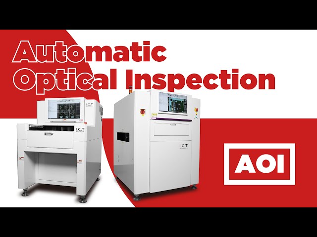
I.C.T Provide SMT Production Line solutions with Automated Optical Inspection (AOI) AOI is short for Automated Optical Inspection, which is widely used in the electronics industry to check the appearance of PCBA assembly at the back end of the cir
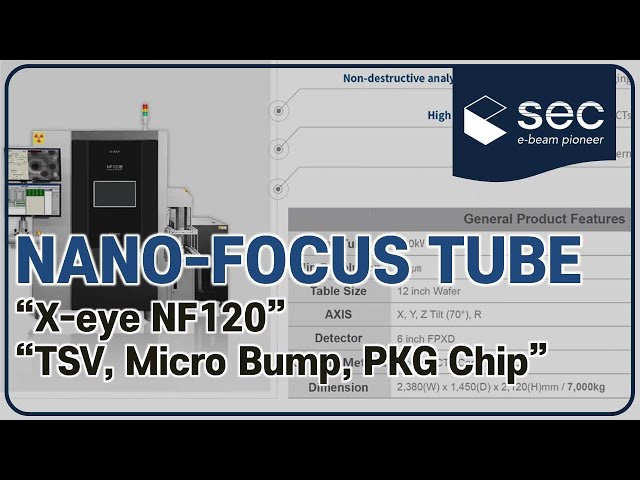
#Xray#Inspection#SEC Nano-focus Tube of 200 nano resolution which is specialized for sub-micron defects of Semiconductor Packaging, Wafer Level Packaging(WLP). -Non-destructive Analysis System -High-Resolution Image with Dual Type CTs -Application
SMTnet Express, July 10, 2014, Subscribers: 22902, Members: Companies: 13928, Users: 36450 Fatigue Damage Behavior of a Surface-mount Electronic Package Under Different Cyclic Applied Loads. Ren Huai-Hui, Wang Xi-Shu - Wind Power Engineer
| http://www.thebranfordgroup.com/dnn3/Auction/BENC0423.aspx
. We provide the names and contact information of available companies solely as a courtesy to our buyers. The Branford Group does not endorse or guarantee the services of any machinery rigging, transport or export company, and cannot be held responsible for any damage, omission or other problems incurred
| https://www.smtfactory.com/pcb-x-ray-inspection-machine
I.C.T Solutions Rising to New Heights: Elevating the PCB X-ray Inspection machine with High-End I.C.T Solutions Views: 0 Author: I.C.T Publish Time: 2023-09-13 Origin: www.smtfactory.com Inquire In the world of advanced electronics manufacturing, the importance of PCB X-ray Inspection Machines cannot be overstated

Nordson Electronics Solutions makes reliable electronics an everyday reality. Our ASYMTEK, MARCH, and SELECT brands deliver precision fluid dispensing, conformal coating, plasma treatment and selective soldering equipment.
2747 Loker Ave West
Carlsbad, USA
Phone: 18002796835

.gif)


