New Equipment | Industrial Automation
Contact: Sandy Lin Email:unity@mvme.cn Skype:onlywnn_1 Telegram:+8618020776786 Mobile(Whatsapp): (+86)-18020776786 QQ :2851195456 Moore Automation Limited Our services Packing & Delivery 1)100% full New! - Original Factory Seal ! 2)War
New Equipment | Industrial Automation
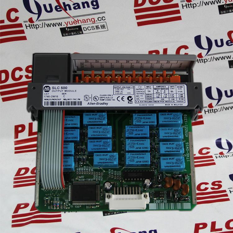
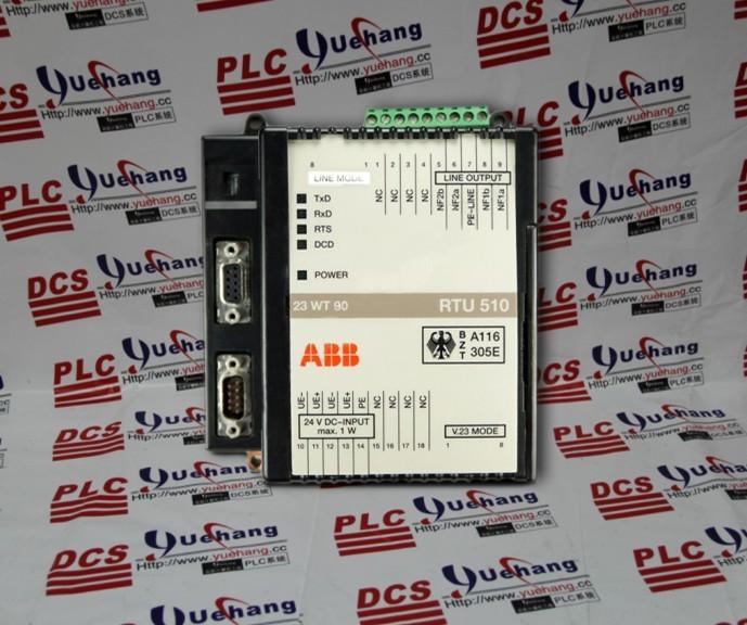
ABB CI615K01 3BSE000756R1 Description: Contact: Sandy Lin Email:unity@mvme.cn Skype:onlywnn_1 Mobile(Whatsapp): (+86)-18020776786 QQ :2851195456 XIAMEN YUEHANG COMPUTER ENGINEERING CO.LTD Our services Packing & Delivery 1)100% full New! -
Electronics Forum | Thu Nov 30 00:41:23 EST 2017 | abhilash4788
Dear All, I have OSP finsh pcb on my production, the pcb thickness is 1.5mm and the product is one sideded pcba. After reflow process, Is there any specific time frame defined for smt completed OSP finish pcba before going for wave soldering proce
Electronics Forum | Sat Sep 08 08:55:24 EDT 2007 | davef
We expect to see a copper shadow along the edge of pads when soldering boards with organic solderability protection [OSP]. IPC-A-610 has defined this as acceptable for years. During early reflow stages, the flux in paste dissolves the OSP where ther
Industry News | 2012-04-13 19:02:54.0
Engineered Conductive Materials, LLC, a leading global supplier of conductive interconnect materials for photovoltaic applications, debuts the fast curing conductive adhesive DB-1590 for use as a solder replacement in next-generation crystalline silicon solar modules using thinned silicon and/or plated bus bars
Technical Library | 2008-04-08 17:42:27.0
Concern about the failure of lead-free BGA packages when portable devices such as cell phones are accidentally dropped and a general concern about the resistance of these packages under shock loading has prompted an interest in the impact strength of the soldered BGA connection. This paper reports the results of the measurement of the impact strength of lead-free 0.5±0.01mm diameter BGA spheres on 0.42mm solder mask defined pads on copper/OSP and ENIG substrates using recently developed equipment that can load individual BGA spheres at high strain rates in shear and tension.
Imagineering, Inc. | https://www.pcbnet.com/blog/how-pcbs-are-made/
. Here’s an overview of that design process. Step 1: Schematic Design Engineers will design schematics that define the purpose of the PCB
Heller Industries Inc. | https://hellerindustries.com/wp-content/uploads/2018/07/last-will-of-bga-void.pdf
, 1.0mm pitch, various solder ball diameters SnPb solder paste Test vehicle one: 2.36mm thick (93 mil), FR-4, 8 internal planes, OSP finish Thermal cycling: 0°C-100


