Industry Directory | Consultant / Service Provider
For nearly 20 years, H&T Global Circuits has gone from the largest printed circuit board (PCB) manufacturer in Florida to one of the largest privately held PCB manufacturers in the world.
Industry Directory | Manufacturer
Manufacturer of advanced process chemistry for plating, masking and stripping. Custom manufacturing of automated equipment for electrodeposion including; hoist systems, reel-to-reel and continuous vertical processing equipment.
Double-Sided & Multi-Layer PCB Material: - FR-4 / Hi-Temp FR-4 / FR-5 / G10 / BT / Polyimide - Very Thin PCB: 0.004" 2L ~ 0.030" 8L - Thick Copper: 1/4 oz. ~ 11 oz. Process: - PTH - Blind/Buried/Segmented Via - Sequential Lamination - MicroVia Capa
New Equipment | Fabrication Services
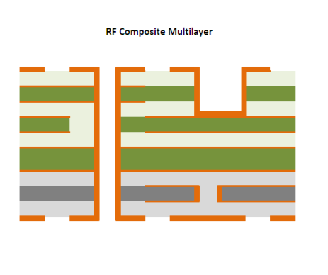
Multilayer PCB's ACI manufactures a wide variety of Multilayer PCB's for various applications spanning numerous industries and technologies. We can build your high layer count PCB's using a wide variety of high speed low loss materials from epoxies
Electronics Forum | Mon Aug 16 20:32:10 EDT 2004 | davef
First, we didn't say "electrolytic soft gold with a minimum thickness of 5-8 of Au". We said, "'electrolytic soft gold' thickness 5 to 8uin". FOCUS. ;-) Second, we're unaware of an industry accepted specification that you can reference. IPC-2221
Electronics Forum | Mon Aug 16 18:09:33 EDT 2004 | Kris
ok I agree there has been a confusion with terminology When you say electrolytic soft gold with a minimum thickness of 5-8 of Au, is there a standard that you spec this from ?
Industry News | 2003-02-07 09:13:12.0
The Sessions Covered Current and Emerging Technologies
Industry News | 2010-09-13 15:36:15.0
IPC — Association Connecting Electronics Industries® has released IPC-1601, Printed Board Handling and Storage Guidelines. The industry's sole standard on the handling, packaging and storage of printed boards, IPC-1601 provides users with guidance on how to protect printed boards from contamination, physical damage, solderability degradation, electrostatic discharge and moisture uptake.
Technical Library | 2014-08-07 15:13:44.0
Gold embrittlement in SnPb solder is a well-known failure mechanism in electronic assembly. To avoid this issue, prior studies have indicated a maximum gold content of three weight percent. This study attempts to provide similar guidance for Pb-free (SAC305) solder. Standard surface mount devices were assembled with SnPb and SAC305 solder onto printed boards with various thicknesses of gold plating. The gold plating included electroless nickel immersion gold (ENIG) and electrolytic gold of 15, 25, 35, and 50 microinches over nickel. These gold thicknesses resulted in weight percentages between 0.4 to 7.0 weight percent.
Technical Library | 2020-08-27 01:22:45.0
Initially adopted internal specifications for acceptance of printed circuit boards (PCBs) used for wire bonding was that there were no nodules or scratches allowed on the wirebond pads when inspected under 20X magnification. The nodules and scratches were not defined by measurable dimensions and were considered to be unacceptable if there was any sign of a visual blemish on wire-bondable features. Analysis of the yield at a PCB manufacturer monitored monthly for over two years indicated that the target yield could not be achieved, and the main reasons for yield loss were due to nodules and scratches on the wirebonding pads. The PCB manufacturer attempted to eliminate nodules and scratches. First, a light-scrubbing step was added after electroless copper plating to remove any co-deposited fine particles that acted as a seed for nodules at the time of copper plating. Then, the electrolytic copper plating tank was emptied, fully cleaned, and filtered to eliminate the possibility of co-deposited particles in the electroplating process. Both actions greatly reduced the density of the nodules but did not fully eliminate them. Even though there was only one nodule on any wire-bonding pad, the board was still considered a reject. To reduce scratches on wirebonding pads, the PCB manufacturer utilized foam trays after routing the boards so that they did not make direct contact with other boards. This action significantly reduced the scratches on wire-bonding pads, even though some isolated scratches still appeared from time to time, which caused the boards to be rejected. Even with these significant improvements, the target yield remained unachievable. Another approach was then taken to consider if wire bonding could be successfully performed over nodules and scratches and if there was a dimensional threshold where wire bonding could be successful. A gold ball bonding process called either stand-off-stitch bonding (SSB) or ball-stitch-on-ball bonding (BSOB) was used to determine the effects of nodules and scratches on wire bonds. The dimension of nodules, including height, and the size of scratches, including width, were measured before wire bonding. Wire bonding was then performed directly on various sizes of nodules and scratches on the bonding pad, and the evaluation of wire bonds was conducted using wire pull tests before and after reliability testing. Based on the results of the wire-bonding evaluation, the internal specification for nodules and scratches for wirebondable PCBs was modified to allow nodules and scratches with a certain height and a width limitation compared to initially adopted internal specifications of no nodules and no scratches. Such an approach resulted in improved yield at the PCB manufacturer.
SMTnet Express, August 7, 2014, Subscribers: 23058, Members: Companies: 13975, Users: 36604 Gold Embrittlement In Lead-Free Solder. Craig Hillman, Nathan Blattau, Joelle Arnold, Thomas Johnston, Stephanie Gulbrandsen; DfR Solutions , Julie Silk
GPD Global | https://www.gpd-global.com/co_website/pdf/GPD-Global-CMRT-2021.xlsx
“Mitsubishi Materials Corporation” 7. Changed “Niotan” to “Kemet Blue Powder” 8. Added “Nihon Material Co. LTD” as a gold refiner 9. Added “Aida Chemical Industries Co
ASYMTEK Products | Nordson Electronics Solutions | https://www.nordson.com/en/divisions/efd/resource-center/solder-glossary-of-terms
. Some typical brazing alloys include copper-zinc, copper-gold, copper-phosphorous, and silver-based alloys. The melting temperatures for brazing alloys range from 450° C (852° F) to 1100° C (2012° F


