New Equipment | Fabrication Services
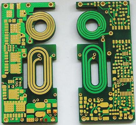
Material: FR-4 Board thickness: 2.4mm Copper thickness: 140um/4oz Surface finishing: Immersion Gold (ENIG) Solder mask: blue, green, yellow, white, red, black, purple Application: UPS, power supply, convertor, motor For your board, feel free t
.jpg)
Layer Count: 8L Board Thickness: 1.0mm Panel Dimension:190*86mm/2up Material: S1141 Copper on board surface: 35μm Min Hole Diameter: 0.1mm Min line Width/Space: 8/8mil Surface Finish: ENIG+Selective OSP in BGA area This quick turn PCB is manufacture
Electronics Forum | Sat Oct 06 08:42:21 EDT 2001 | davef
Please give us additional background on your board, solder, process, etc. If you are talking about black pad in ENIG solderability preservative, check the fine SMTnet archives to get started.
Electronics Forum | Mon Jun 17 13:45:29 EDT 2002 | genny
When the pad comes off, is it leaving behind a "black" area? Your board may be suffering from black pad - a condition that occasionally affects ENIG finish boards. It is a process control issue with your board fabricator. The nickel is oxidising b
Technical Library | 2013-01-17 15:34:33.0
The use of an electroless nickel, immersion gold (ENIG) surface finish comes with the inherent potential risk of Black Pad failures that can cause fracture embrittlement at the interface between the solder and the metal pad. As yet, there is no conclusive agreed solution to effectively eliminate Black Pad failures. The case studies presented are intended to add to the understanding of the Black Pad failure mechanism and to identify both the plating and the subsequent assembly processes and conditions that can help to prevent the likelihood of Black Pad occurring.
smeared solder paste pattern. A typical pad size for
Heller Industries Inc. | https://hellerindustries.com/wp-content/uploads/2018/07/last-will-of-bga-void.pdf
] Investigation Specifics: 84 I/O Plastic CSP, daisy chained, 0.3mm (12 mil) diameter solderballs Sn63 solder paste Test vehicle: Characteristics not available, Immersion Silver (IAg) and ENIG finishes Thermal cycling: 0°C-100
PCB Libraries, Inc. | https://www.pcblibraries.com/forum/ipc7093a-btc-qfn-solder-mask-defined-thermal-pad_topic2154_post11220.html
causing solder protrusion. 2. When the solder goes into the vias, it robs the thermal pad from having the optimal solder joint. Less solder = bad connection. 3. The thinner PCB thickness of 1 mm can be problematic because it's easier for the solder to flow out the bottom side and could cause shorting


