New Equipment | Cleaning Agents
MICRONOX MX2100 is an aqueous, single-phase solvent designed to remove tough flux residue from PMIC devices including IGBT modules and power MOSFETs. MX2100 has a well-balanced formula that provides outstanding cleaning performance and metal compatib
Design For Manufacturability And Yield Enhancement. The Design for Manufacturability (DFM) engine searches for fabrication issues and discovers areas where yields may be increased. GraphiCode's Contour Technology produces fast and accurate results f
Electronics Forum | Sun Sep 12 08:30:29 EDT 2004 | davef
Well, another alternative is to use a water washable flux. If you insist on staying with a NC flux, use one that is probable. We prefer to probe solder, rather than copper.
Electronics Forum | Tue Jun 05 21:14:10 EDT 2001 | davef
You aren't going to post our stuff on your "Hey, I'm the wizard site", are you? Board fab, Pad coatings, OSP 1 OSPs: Imidazole (Via Systems) is good. Entek (Enthone) works, but requires strict thickness control in fab. 2 Enthone CU56 allows one t
Industry News | 2019-03-10 20:30:11.0
The proliferation of tighter microvia densities and signal integrity requirements in printed boards within the electronics industry has revealed reliability concerns with microvia structures in high performance products. A number of IPC OEM member companies have approached IPC with examples of microvia failures in high-profile hardware that were not observed until after bare printed board fabrication, inspection and acceptance, including:
Industry News | 2019-11-05 22:07:01.0
Tenting a via refers to covering via with soldermask to enclose or skin over the opening. A via is a hole drilled into the PCB that allows multiple layers on the PCB to be connected to each other. A non tented via is just a via that is not covered with the soldermask layer. Leaving these vias exposed or covered has pros and cons depending on the your design and manufacturing requirements.
Parts & Supplies | Repair/Rework
Repair parts include: CPU circuit board repair and maintenance of the I / O board, servo circuit board repair, the image processing circuit board repair, industrial CCD camera repair, frequency converter repair, PLC repair, touch screen repair, laser
Technical Library | 2015-02-19 16:54:34.0
Pad cratering is an important failure mode besides crack of solder joint as it’ll pass the regular test but have impact on the long term reliability of the product. A new pin pull test method with solder ball attached and positioning the test board at an angle of 30º is employed to study the strength of pad cratering. This new method clearly reveals the failure mechanism. And a proper way to interpret the finite element analysis (FEA) result is discussed. Impact of pad dimension, width and angle of copper trace on the strength is included. Some findings not included in previous research could help to guide the design for better performance
Technical Library | 2020-08-27 01:22:45.0
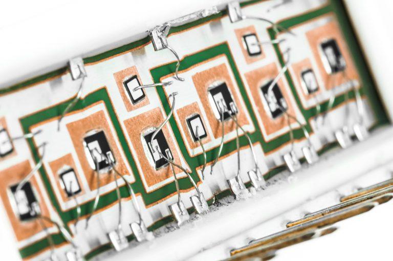
Initially adopted internal specifications for acceptance of printed circuit boards (PCBs) used for wire bonding was that there were no nodules or scratches allowed on the wirebond pads when inspected under 20X magnification. The nodules and scratches were not defined by measurable dimensions and were considered to be unacceptable if there was any sign of a visual blemish on wire-bondable features. Analysis of the yield at a PCB manufacturer monitored monthly for over two years indicated that the target yield could not be achieved, and the main reasons for yield loss were due to nodules and scratches on the wirebonding pads. The PCB manufacturer attempted to eliminate nodules and scratches. First, a light-scrubbing step was added after electroless copper plating to remove any co-deposited fine particles that acted as a seed for nodules at the time of copper plating. Then, the electrolytic copper plating tank was emptied, fully cleaned, and filtered to eliminate the possibility of co-deposited particles in the electroplating process. Both actions greatly reduced the density of the nodules but did not fully eliminate them. Even though there was only one nodule on any wire-bonding pad, the board was still considered a reject. To reduce scratches on wirebonding pads, the PCB manufacturer utilized foam trays after routing the boards so that they did not make direct contact with other boards. This action significantly reduced the scratches on wire-bonding pads, even though some isolated scratches still appeared from time to time, which caused the boards to be rejected. Even with these significant improvements, the target yield remained unachievable. Another approach was then taken to consider if wire bonding could be successfully performed over nodules and scratches and if there was a dimensional threshold where wire bonding could be successful. A gold ball bonding process called either stand-off-stitch bonding (SSB) or ball-stitch-on-ball bonding (BSOB) was used to determine the effects of nodules and scratches on wire bonds. The dimension of nodules, including height, and the size of scratches, including width, were measured before wire bonding. Wire bonding was then performed directly on various sizes of nodules and scratches on the bonding pad, and the evaluation of wire bonds was conducted using wire pull tests before and after reliability testing. Based on the results of the wire-bonding evaluation, the internal specification for nodules and scratches for wirebondable PCBs was modified to allow nodules and scratches with a certain height and a width limitation compared to initially adopted internal specifications of no nodules and no scratches. Such an approach resulted in improved yield at the PCB manufacturer.
| https://www.smtfactory.com/I-C-T-V5000H-SMT-On-line-Automated-Optical-Inspection-AOI-Machine-for-SMT-Line-pd49400944.html
+Telecentric lens The high component solder joint inspection is not affected as no shadow effect in the entire field of view. Entire FOV Assist Position High detection ability on no exposed pad components(BGA,etc
ASYMTEK Products | Nordson Electronics Solutions | https://www.nordson.com/en/divisions/dage/test-types/first-bond-ball-pull-stud-bump-pull
. First bond ball pull utilises cold bump pull jaw technology to apply a vertical load (a pull test) to ball bonds and stud bumps. Ball shear tests can sometimes promote pad cratering due to the aggressive nature of the bonding process which can weaken the ball bonds

COT specializes in high quality SMT nozzles and consumables for pick and place machines. We provide special engineering design service of custom nozzles for those unique and odd components.
2481 Hilton Drive
Gainesville, GA USA
Phone: (770) 538-0411


