
Industry Directory | Training Provider / Manufacturer's Representative / Equipment Dealer / Broker / Auctions / Consultant / Service Provider
Products, services, training & consulting for the assembly, rework & repair of electronic assemblies. BGA process experts. Manufacturers Rep, Distributor & Service Provider for Seamark/Zhuomao and Shuttle Star BGA Rework Stations.
Industry Directory | Manufacturer
a pcb manufacturer in China specializing in multi-layer pcbs that meet RoHs, UL, IPC standards.
New Equipment | Assembly Services
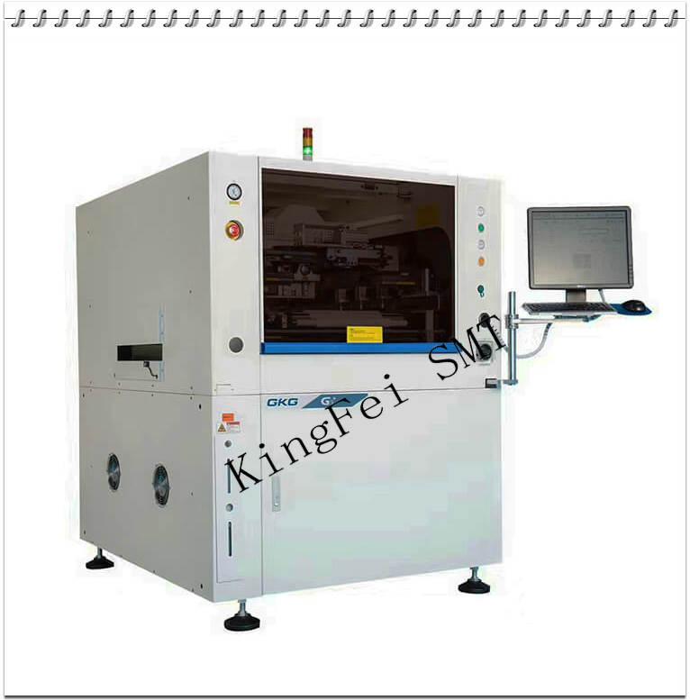
G9 + automatic vision printing machine is a new product for SMT high-end application field, which can perfectly meet the process requirements of 03015, 0.25pich and other fine spacing, high precision and high speed. Introduction to standard function
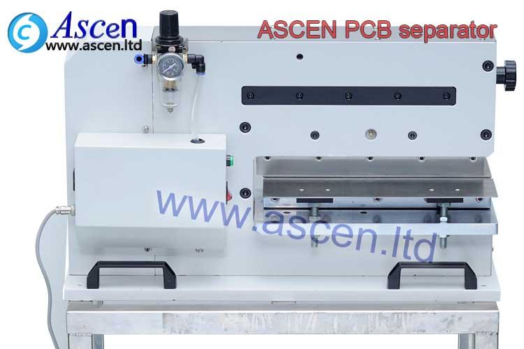
auto PCB cutting machine For internal strength generates during separation, Minimize it to value under 180uE ,to avoid PCB solder crack or component damage ASCEN technology as the PCB separator manufacturer provide all kinds of PCB cutting machine
Electronics Forum | Fri Feb 28 08:48:00 EST 2020 | SMTA-Joe
We've made the decision to move towards Gold Immersion on our PCBs to eliminate flatness issues with QFNs and BGAs. Land/component pad geometry, population density, and other factors, have made it necessary to ensure a near perfectly flat surface tha
Electronics Forum | Fri Mar 20 05:55:24 EDT 2020 | yuaanliie
The gold plating on PCB has a 40% higher resistivity, and it is much more expensive. So gold is not used instead of copper for conductors. Last month I purchased some PCB from Cplfpc and Greatpcb.
Industry News | 2003-05-19 10:06:43.0
The PCB is available with a maximum panel size of 406-by-460mm and a minimum board thickness of 0.8mm.
Industry News | 2013-06-07 15:41:36.0
IPC Study of Quality Benchmarks for the Electronics Manufacturing Services (EMS) Industry for 2013 is now available from IPC — Association Connecting Electronics Industries®. T
Parts & Supplies | Pick and Place/Feeders
We can supply you the following UNIVERSAL Feeders. Also Feeder Parts, Feeder Storage Carts / Feeder Trolley, Feeder Calibration Jig. 49889209 8mm High Performance DL-60 (Gold Plus) 49889210 8mm High Performance DL-60 (Gold Plus) 49889211 8mm High

Parts & Supplies | Visual Inspection
We can supply you the following UNIVERSAL Feeders. Also Feeder Parts, Feeder Storage Carts / Feeder Trolley, Feeder Calibration Jig. 49889209 8mm High Performance DL-60 (Gold Plus) 49889210 8mm High Performance DL-60 (Gold Plus) 49889211 8mm High
Technical Library | 2021-07-20 20:02:29.0
During the manufacturing of printed circuit boards (PCBs) for a Flight Project, it was found that a European manufacturer was building its boards to a European standard that had no requirement for copper wrap on the vias. The amount of copper wrap that was measured on coupons from the panel containing the boards of interest was less than the amount specified in IPC-6012 Rev B, Class 3. To help determine the reliability and usability of the boards, three sets of tests and a simulation were run. The test results, along with results of simulation and destructive physical analysis, are presented in this paper. The first experiment involved subjecting coupons from the panels supplied by the European manufacturer to thermal cycling. After 17 000 cycles, the test was stopped with no failures. A second set of accelerated tests involved comparing the thermal fatigue life of test samples made from FR4 and polyimide with varying amounts of copper wrap. Again, the testing did not reveal any failures. The third test involved using interconnect stress test coupons with through-hole vias and blind vias that were subjected to elevated temperatures to accelerate fatigue failures. While there were failures, as expected, the failures were at barrel cracks. In addition to the experiments, this paper also discusses the results of finite-element analysis using simulation software that was used to model plated-through holes under thermal stress using a steady-state analysis, also showing the main failure mode was barrel cracking. The tests show that although copper wrap was sought as a better alternative to butt joints between barrel plating and copper foil layers, manufacturability remains challenging and attempts to meet the requirements often result in features that reduce the reliability of the boards. Experimental and simulation work discussed in this paper indicate that the standard requirements for copper wrap are not contributing to the overall board reliability, although it should be added that a design with a butt joint is going to be a higher risk than a reduced copper wrap design. The study further shows that procurement requirements for wrap plating thickness from Class 3 to Class 2 would pose little risk to reliability (minimum 5 μm/0.197 mil for all via types).Experimental results corroborated by modeling indicate that the stress maxima are internal to the barrels rather than at the wrap location. In fact, the existence of Cu wrap was determined to have no appreciable effect on reliability.
Technical Library | 2020-08-27 01:22:45.0
Initially adopted internal specifications for acceptance of printed circuit boards (PCBs) used for wire bonding was that there were no nodules or scratches allowed on the wirebond pads when inspected under 20X magnification. The nodules and scratches were not defined by measurable dimensions and were considered to be unacceptable if there was any sign of a visual blemish on wire-bondable features. Analysis of the yield at a PCB manufacturer monitored monthly for over two years indicated that the target yield could not be achieved, and the main reasons for yield loss were due to nodules and scratches on the wirebonding pads. The PCB manufacturer attempted to eliminate nodules and scratches. First, a light-scrubbing step was added after electroless copper plating to remove any co-deposited fine particles that acted as a seed for nodules at the time of copper plating. Then, the electrolytic copper plating tank was emptied, fully cleaned, and filtered to eliminate the possibility of co-deposited particles in the electroplating process. Both actions greatly reduced the density of the nodules but did not fully eliminate them. Even though there was only one nodule on any wire-bonding pad, the board was still considered a reject. To reduce scratches on wirebonding pads, the PCB manufacturer utilized foam trays after routing the boards so that they did not make direct contact with other boards. This action significantly reduced the scratches on wire-bonding pads, even though some isolated scratches still appeared from time to time, which caused the boards to be rejected. Even with these significant improvements, the target yield remained unachievable. Another approach was then taken to consider if wire bonding could be successfully performed over nodules and scratches and if there was a dimensional threshold where wire bonding could be successful. A gold ball bonding process called either stand-off-stitch bonding (SSB) or ball-stitch-on-ball bonding (BSOB) was used to determine the effects of nodules and scratches on wire bonds. The dimension of nodules, including height, and the size of scratches, including width, were measured before wire bonding. Wire bonding was then performed directly on various sizes of nodules and scratches on the bonding pad, and the evaluation of wire bonds was conducted using wire pull tests before and after reliability testing. Based on the results of the wire-bonding evaluation, the internal specification for nodules and scratches for wirebondable PCBs was modified to allow nodules and scratches with a certain height and a width limitation compared to initially adopted internal specifications of no nodules and no scratches. Such an approach resulted in improved yield at the PCB manufacturer.
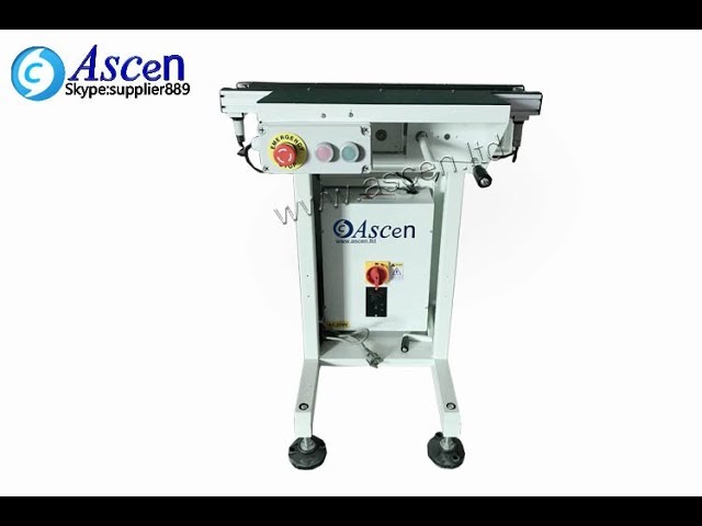
https://www.ascen.ltd/Products/Automatic_SMT_equipment/PCB_conveyor/100.html PCB linking conveyor and PCB belt conveyor mainly used to connect different type PCB board handing equipment effectively for the SMT production line. ASCEN technology is ava
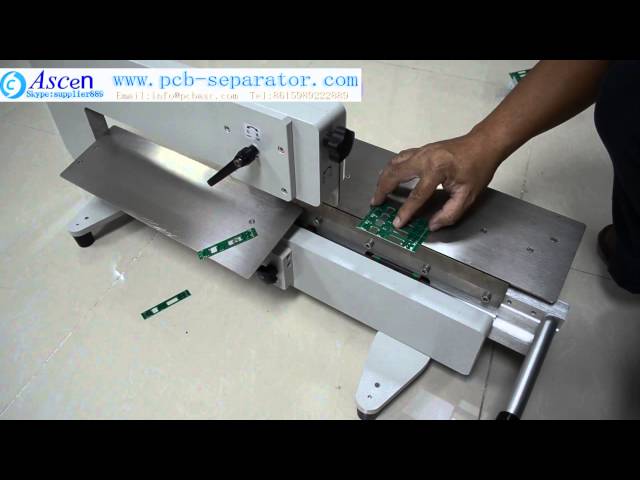
http://www.pcb-separator.com/ https://www.pcb-separator.com/html/PRODUCTS/PCB%20separator/2019/1113/832.html Hand push pcb cutter/PCB cutting machine manufacturer/PCB V-cut machine manufacturer/PCB depaneling equipment, automatic pcb cutting machine,
Training Courses | | | PCB Rework and Hand Soldering Courses
The PCB rework and hand soldering courses courses cover techniques of rework and repair of PCBs, BGAs and other electronics assemblies, and teach fundamentals of soldering of electronics assemblies.
Career Center | Houston, Texas USA | Engineering,Management,Quality Control,Technical Support
Seasoned Process & Quality Engineer. Degreed Chemical Engineer. 20+ years in Electronics Semiconductor manufacturing. Proficient in Quality Statistical tools, Design of Experiments, FMEAs, APQP, PPAP, ISO 9000, ISO/TS 16949 etc.
Career Center | Erode, Tamilnadu India | Engineering
Professional Summary 3+ years of experience in the PCB CAM engineering Exposure to FRONTLINE GENESIS 2000 Having exposure in UCAM Exposure to Create, Array & Panelize it for manufacturability Experienced in Creating impedance cou
| https://www.eptac.com/faqs/ask-helena-leo/ask/failing-to-remove-gold-plating-in-final-assembly
: If the gold plating on the surface of via holes is not removed from the printed circuit boards, does this constitute a defect or failure of the
Imagineering, Inc. | https://www.pcbnet.com/blog/when-to-use-fr4-printed-circuit-boards/
. The glass transition (TG) for FR4 is between 115ºC and 200ºC depending on the manufacture. Standard FR4 has a lower TG of 140ºC to 150ºC, while HighTG FR4 is usually around
Products, services, training & consulting for the assembly, rework & repair of electronic assemblies. BGA process experts. Manufacturers Rep, Distributor & Service Provider for Seamark/Zhuomao and Shuttle Star BGA Rework Stations.
Training Provider / Manufacturer's Representative / Equipment Dealer / Broker / Auctions / Consultant / Service Provider
1750 Mitchell Ave.
Oroville, CA USA
Phone: (888) 406-2830


