Industry Directory | Manufacturer
Nepes offers flip chip solutions ranging from wafer bumping to advanced packaging and testing for IC manufactures, module electronics and end-product makers.

Aluminum Wirebonding Gold Wirebonding Gold Ribbonbonding Wafer Bumping Flip Chip Packaging BGA LGA SMT Direct Chip Attach System In Package Hybrid MCM Stacked Die 3D Packaging 3D Memory Rad Hard RF Packaging
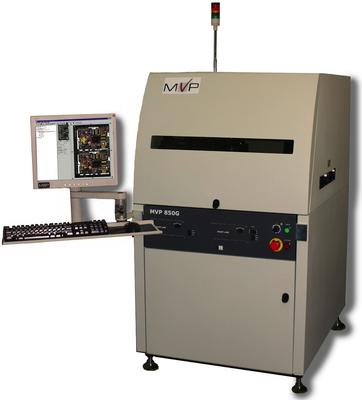
Microelectronics and Semiconductor Inspection. MVP's 850G provides the highest accuracy flip-chip, die assembly inspection. Ensuring the correct placement of the die on the substrate, while providing edge, FM and surface inspection. The 850G modu
Electronics Forum | Wed Sep 07 17:14:11 EDT 2005 | GS
finest pitch requires ball bonding (gold) GS
Electronics Forum | Thu Sep 08 07:04:02 EDT 2005 | davef
Finer pitch: Wedge bonding can be designed and manufactured to very small dimensions, down to 50 mm pitch. Processing speed: Machine rotational movements make the overall speed of the wedge bonding process less than thermosonic ball bonding. Alumin
Industry News | 2013-10-25 16:15:31.0
Barry Industries introduces a new 0904 size chip attenuator for Ku, K and Ka bands. The AV0904GA attenuator has been characterized to 30GHz, features gold wirebondable I/O terminals with epoxy mount ground pads and is rated to 750mW.
Industry News | 2012-09-10 19:45:44.0
San Francisco Circuits is now offering Micro-Circuits.
Technical Library | 2020-08-27 01:22:45.0
Initially adopted internal specifications for acceptance of printed circuit boards (PCBs) used for wire bonding was that there were no nodules or scratches allowed on the wirebond pads when inspected under 20X magnification. The nodules and scratches were not defined by measurable dimensions and were considered to be unacceptable if there was any sign of a visual blemish on wire-bondable features. Analysis of the yield at a PCB manufacturer monitored monthly for over two years indicated that the target yield could not be achieved, and the main reasons for yield loss were due to nodules and scratches on the wirebonding pads. The PCB manufacturer attempted to eliminate nodules and scratches. First, a light-scrubbing step was added after electroless copper plating to remove any co-deposited fine particles that acted as a seed for nodules at the time of copper plating. Then, the electrolytic copper plating tank was emptied, fully cleaned, and filtered to eliminate the possibility of co-deposited particles in the electroplating process. Both actions greatly reduced the density of the nodules but did not fully eliminate them. Even though there was only one nodule on any wire-bonding pad, the board was still considered a reject. To reduce scratches on wirebonding pads, the PCB manufacturer utilized foam trays after routing the boards so that they did not make direct contact with other boards. This action significantly reduced the scratches on wire-bonding pads, even though some isolated scratches still appeared from time to time, which caused the boards to be rejected. Even with these significant improvements, the target yield remained unachievable. Another approach was then taken to consider if wire bonding could be successfully performed over nodules and scratches and if there was a dimensional threshold where wire bonding could be successful. A gold ball bonding process called either stand-off-stitch bonding (SSB) or ball-stitch-on-ball bonding (BSOB) was used to determine the effects of nodules and scratches on wire bonds. The dimension of nodules, including height, and the size of scratches, including width, were measured before wire bonding. Wire bonding was then performed directly on various sizes of nodules and scratches on the bonding pad, and the evaluation of wire bonds was conducted using wire pull tests before and after reliability testing. Based on the results of the wire-bonding evaluation, the internal specification for nodules and scratches for wirebondable PCBs was modified to allow nodules and scratches with a certain height and a width limitation compared to initially adopted internal specifications of no nodules and no scratches. Such an approach resulted in improved yield at the PCB manufacturer.
Career Center | , Philippines | Engineering,Technical Support
Electronic manufacturing and Semiconductor equipment programming, sustenance and preventive maintenance. Knowledge in PLC, pneumatics and automated equipment. Desktop, Laptop computer servicing trouble-shooting, repair, hardware and software instal
Career Center | , | 2013-03-07 10:18:07.0
Currently work as Equipment Engineer at Integrated Microelectronics Inc., Philippines handles Line Maintenance Technicians, that performs production equipment setup and sustenance. Implements/creates improvements on assigned area. Maintains group KRA


