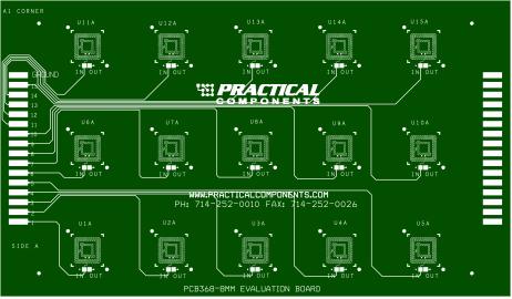
PC boards and kits for machine set-up and calibration, hand solder training, rework, practice, testing and more along with a drawing of each PCB. Practical has a PCB board or kit to meet your requirements. BGA Fine Pitch, Global Daisy-Chain or Vari
New Equipment | Board Handling - Pallets,Carriers,Fixtures
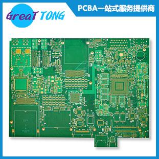
Supplier: Shenzhen Grande Electronics Layers: 4 Application: Grande - Automobile PCB Prototyping and Manufacturing PCB Parameter: FR-4/HTG150 Thickness: 1.6mm Surface Treatment: ENIG Testing: 100% E-test Package: Vacuum packing Lead Time: 10-15 da
Electronics Forum | Mon Feb 12 17:05:29 EST 2007 | Jose
Today is more complicate to find components with lead than with "lead free", and the, I think that you have very feww lead components. And, if don�t work on exceptionals companies, you MUST use LEAD FREE PASTE. In one case, or in the opposite, the re
Electronics Forum | Mon Feb 19 15:32:42 EST 2007 | blnorman
We use SnPb paste and bar with leaded and non-leaded component finishes. The predominant finish on components we use is Tin, there are a few NiPdAu. We've had no problems with the component finishes used in the SnPb process.
Industry News | 2003-05-29 08:30:31.0
Losses halved in the first half year � New organization of electronics group next on the agenda
Industry News | 2012-04-06 16:02:03.0
When a component manufacturer discontinues a particular component, it creates a ripple effect throughout the electronics assembly industry, leaving EMS providers with myriad critical questions to answer.
Technical Library | 2012-03-22 20:40:01.0
Miniaturization continues to be a driving force in both integrated circuit packaging and printed circuit board laminate technology. In addition to decreasing component pitch (lead to lead spacing), utilization of the vertical space by stacking packages ha
Technical Library | 2024-01-15 20:45:42.0
Miniaturization continues to be a driving force in both integrated circuit packaging and printed circuit board laminate technology. In addition to decreasing component pitch (lead to lead spacing), utilization of the vertical space by stacking packages has found wide acceptance by both designers and manufactures of electronics alike. Lead free Package on Package (PoP) technology represents one of the latest advancements in vertical electronics packaging integration and has become the preferred technology for mobile hand held electronics applications. TT Electronics in Perry, Ohio has developed the capability to assemble and rework numerous "state of the art" packaging technologies. This paper will focus on the essential engineering development activities performed to demonstrate TT Electronics' ability to both assemble and rework PoP components.
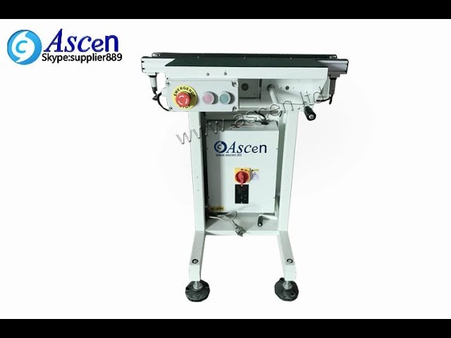
https://www.ascen.ltd/Products/Automatic_SMT_equipment/PCB_conveyor/100.html PCB linking conveyor and PCB belt conveyor mainly used to connect different type PCB board handing equipment effectively for the SMT production line. ASCEN technology is ava
https://www.ascen.ltd/Products/Automatic_SMT_equipment/PCB_conveyor/100.html PCB linking conveyor and PCB belt conveyor mainly used to connect different type PCB board handing equipment effectively for the SMT production line. ASCEN technology is ava
HASL - WHAT A HASSLE, or HASL'd AGAIN. If you don't see the images, please visit online version at #Application.SmtNet.baseURL#/express/ Featured Article HASL - WHAT A HASSLE, or HASL'd AGAIN. Proof Of Design MoonMan This article updates
Evaluation of Laminates in Pb-free HASL Process and Pb-free Assembly Environment SMTnet Express September 20, 2012, Subscribers: 25503, Members: Companies: 8989, Users: 33687 Evaluation of Laminates in Pb-free HASL Process and Pb-free Assembly
ASYMTEK Products | Nordson Electronics Solutions | https://www.nordson.com/en/divisions/yestech/about-nordson-yestech/articles/combining-2d-and-3d-aoi-the-most-effective-inspection
. Coplanarity issues are also prevalent on smaller chip components (i.e.01005), leaded devices and BGA packaged devices. In order to attain the highest level of quality assurance (QA
Imagineering, Inc. | https://www.pcbnet.com/blog/the-role-of-pcb-assembly-and-fabrication-in-the-aerospace-industry/
. This parameter describes the relationship between the size of the board and its circuits, which should be no more than 1:10. The general purpose of a PCB is to transfer electricity between its components, and one way to do that is to add more layers

COT specializes in high quality SMT nozzles and consumables for pick and place machines. We provide special engineering design service of custom nozzles for those unique and odd components.
2481 Hilton Drive
Gainesville, GA USA
Phone: (770) 538-0411


