Industry Directory | Consultant / Service Provider / Distributor / Manufacturer / Other
Ludee Circuits offer RoHS PCB.We could offer leadfree HASL,Entek, flash gold, immersion gold, immersion silver, immersion tin finishing based on standard FR-4, CEM-3 materials, Teflon, Rogers RO4000 series, as well as high Tg S1170 materials.
Industry Directory | Manufacturer
US manufacturer of metallized ceramic substrates & packages; specializing in PCTF (plated copper over thick film) & low cost AgENIG (silver with electroless nickel and immersion gold plating).
New Equipment | Assembly Services
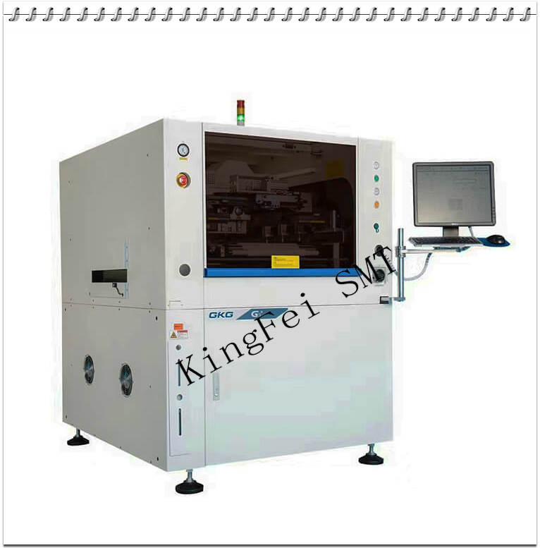
G9 + automatic vision printing machine is a new product for SMT high-end application field, which can perfectly meet the process requirements of 03015, 0.25pich and other fine spacing, high precision and high speed. Introduction to standard function

New Equipment | Assembly Services
Product features: The servo system is convenient and accurate for positioning. The Japanese THK guide rail and Taiwan STK variable frequency motor are used to drive the scraper base to ensure the printing accuracy. The printing scraper can be rota
Electronics Forum | Thu Oct 07 20:34:48 EDT 1999 | Tony Huang
Hi, Does anybody know what is the minimum gold plating thickness on the PCB goldfinger required by the industrial specifications - IPC, Bellcore, etc. Where can I find the information? Appreciate for the help! Thanks, Tony
Electronics Forum | Fri Oct 08 17:12:31 EDT 1999 | Dave F
| Hi, | | Does anybody know what is the minimum gold plating thickness on the PCB goldfinger required by the industrial specifications - IPC, Bellcore, etc. Where can I find the information? Appreciate for the help! | | Thanks, | Tony | Hi Tony:
Used SMT Equipment | Screen Printers
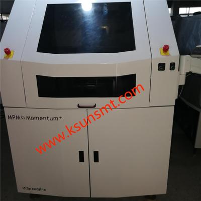
MPM Momentum+ Printer Substrate treatment Maximum plate size(XxY) 609.6 mm x 508 mm(24”x 20”) Segmented mode-Momentum Elite 457 mm x 508 mm(18"x20") Minimum Plate Size (XxY)
Used SMT Equipment | Screen Printers
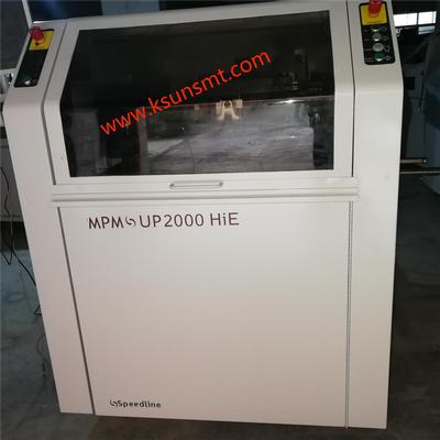
MPM UP2000HiE PRINTER Substrate treatment Minimum/maximum size 2"x 2"(50.0 mm x50.0 mm) to 20" x 16" (508 mm x 406 mm)(16 "or larger substrate requires special clamps) Thickness rang
Industry News | 2003-05-19 10:06:43.0
The PCB is available with a maximum panel size of 406-by-460mm and a minimum board thickness of 0.8mm.
Industry News | 2019-05-16 01:27:23.0
There are several surface treatment for PCB board: bare board (no treatment on the surface), rosin board, OSP (Organic Solderability Preservatives), HASL (lead tin, lead-free tin), plating gold, immersion gold, etc., these are relatively conscious treatment. Many people can't tell the difference between plating gold and immersion gold, thinking that it is the same thing, it is a big mistake. The following is a brief introduction to the difference between plating gold and immersion gold.
Parts & Supplies | Circuit Board Assembly Products
PULANG TECHNOLOGY CO,.LTDOffers electronic manufacturing services including PCB designing, electronic contract manufacturing including electronic product design, electronic product development, electronic product repair, PCB manufacturing, electronic
Parts & Supplies | Circuit Board Assembly Products
Specifications 1.One-stop OEM pcb assembly service. 2.ROHS, SGS, UL certificated 3.Reasonable price 4.High Quality 5.Fast Delivery PCB Assembly&PCBA Service 1. Experienced components sourcing team specially for scarce parts 2.1 to 12 layers m
Technical Library | 2014-08-07 15:13:44.0
Gold embrittlement in SnPb solder is a well-known failure mechanism in electronic assembly. To avoid this issue, prior studies have indicated a maximum gold content of three weight percent. This study attempts to provide similar guidance for Pb-free (SAC305) solder. Standard surface mount devices were assembled with SnPb and SAC305 solder onto printed boards with various thicknesses of gold plating. The gold plating included electroless nickel immersion gold (ENIG) and electrolytic gold of 15, 25, 35, and 50 microinches over nickel. These gold thicknesses resulted in weight percentages between 0.4 to 7.0 weight percent.
Technical Library | 2020-07-22 19:39:05.0
The PWB industry needs to complete reliability testing in order to define the minimum copper wrap plating thickness requirement for confirming the reliability of PTH structures. Predicting reliability must ensure that the failure mechanism is demonstrated as a wear-out failure mode because a plating wrap failure is unpredictable. The purpose of this study was to quantify the effects of various copper wrap plating thicknesses through IST testing followed by micro sectioning to determine the failure mechanism and identify the minimum copper wrap thickness required for a reliable PWB. Minimum copper wrap plating thickness has become an even a bigger concern since designers started designing HDI products with buried vias, microvias and through filled vias all in one design. PWBs go through multiple plating cycles requiring planarization after each plating cycle to keep the surface copper to a manageable thickness for etching. The companies started a project to study the relationship between Copper wrap plating thickness and via reliability. The project had two phases. This paper will present findings from both Phase 1 and Phase 2.

http://www.pcb-separator.com/plus/view.php?aid=86 PCB multi cutter machine/high efficiency PCB depaneling 900 machine/ PCB separator
http://www.pcb-separator.com/plus/view.php?aid=86 PCB multi cutter machine/high efficiency PCB depaneling 900 machine/ PCB separator
Training Courses | ON DEMAND | | IPC-6012 Trainer (CIT)
The Certified IPC-6012 Trainer (CIT) courses recognize individuals as qualified trainers in the area of design, fabrication and inspection of rigid printed boards and prepare them to deliver Certified IPC-6012 Specialist (CIS) training.
Events Calendar | Wed Mar 18 00:00:00 EDT 2020 - Wed Mar 18 00:00:00 EDT 2020 | College Park, Maryland USA
CALCE Reliability Science Symposium - Spring 2020
Career Center | Erode, Tamilnadu India | Engineering
Professional Summary 3+ years of experience in the PCB CAM engineering Exposure to FRONTLINE GENESIS 2000 Having exposure in UCAM Exposure to Create, Array & Panelize it for manufacturability Experienced in Creating impedance cou
Career Center | Shen Zhen, China | Management,Sales/Marketing
Working in GLORYPCB for 10 years.knowing electronic supply chain very well. especially for PCB PCBA assembly and other Electronic Manufacturing Service.Glorypcb is a professional electronic manufacturer located in Shenzhen with three facilities.offe
SMT Express, Issue No. 2 - from SMTnet.com Volume 1, Issue No. 2 Wednesday, July 14, 1999 Featured Article Continued From Previous Page PRINTED CIRCUIT BOARD FABRICATION BASICS AN OUTLINE Earl Moon Proof Of Design (POD) 8. PLATING (AND
Imagineering, Inc. | https://www.pcbnet.com/quote/board-quote-taiwan/
Black Blue Red GoldFingers * Gold Finger Plating Thickness No Gold Fingers 10u" 20u" 30u" 50u" Routing Individual Scoring Route/Retain Route/Retain/Scoring Cutouts/Slots
Surface Mount Technology Association (SMTA) | https://www.smta.org/knowledge/proceedings_abstract.cfm?PROC_ID=5255
) when the solder gold content exceeds 5% by weight. Controlling the component gold plating thickness as well as the soldering process temperature and time can prevent gold embrittlement


