Industry Directory | Consultant / Service Provider / Distributor / Events Organizer / Manufacturer / Manufacturer's Representative / Other
Packagly is a custom packaging company , who help clients to grow their business .They are also helping them to create mark in the market
Industry Directory | Manufacturer's Representative
When it comes to packaging, Tycoon Packaging is your one-stop shop. We offer various custom packaging solutions for businesses of all sizes, from small startups to large corporations.

New Equipment | Assembly Services
Product features: The servo system is convenient and accurate for positioning. The Japanese THK guide rail and Taiwan STK variable frequency motor are used to drive the scraper base to ensure the printing accuracy. The printing scraper can be rota
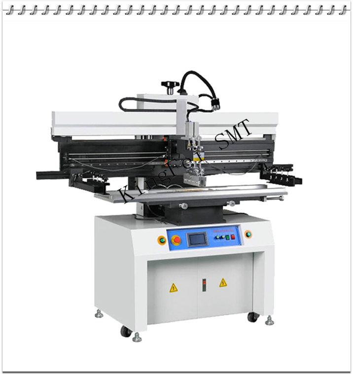
technical parameter Model: s1200 (special type for LED light bar) Overall dimension (L × w × h): 1650 × 620 × 1550 (mm) Platform size: 320 × 1300 (mm) PCB size: 250 × 1250 (mm) Applicable template size: 550 ×
Electronics Forum | Tue Jun 06 20:02:55 EDT 2000 | Dave F
Ravi: I agree with travis. What's the issue?
Electronics Forum | Fri Jun 02 19:43:40 EDT 2000 | Ravi Bhat
One of my customers has asked about concerns, comments, ideas about putting 0402 packages on bottom side of the board. The process will be no clean with reflow/reflow. If anybody out there has some experience or concerns please comment. Regards
Used SMT Equipment | Pick and Place/Feeders
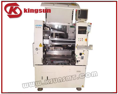
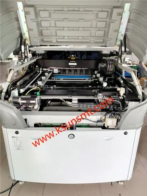
Product number: KE - 2010L Products in detail Substrate size: Min: 50 mmx30mm Max: 330mmx250mm Substrate thickness: Min: 0.4 mm Max: 4 mm Element size: 0402 ~ 20 mm square elementor 26.5 X11mm Mount speed: 11000 CPH SMT precision: 0.05 MM Elem
Used SMT Equipment | Screen Printers
DEK Horizon 03i automatic stencil printer Specification : DEK Horizon 03i High Precision Automatic Solder Paste Printer designed for high precision steel mesh printing or stencil printing in SMT industry. Printing PCB size: 50x50mm to 508x510mm;
Industry News | 2013-08-15 20:58:22.0
Heller Industries announced today that they have entered into a joint development agreement with International Business Machines Corporation (NYSE: IBM), to collaborate on the development of fluxless mass reflow furnace equipment and process for high volume manufacturing. The fluxless process utilizes gas phase formic acid to replace standard fluxing agents, and eliminates the need for pre-reflow fluxing and post-reflow flux cleanup steps.
Industry News | 2011-02-17 15:04:54.0
GPD Global will highlight its Positive Cavity Displacement (PCD) Dispensing in Booth #27 at the upcoming IMAPS Device Packaging conference and exhibition, scheduled to take place March 8-9, 2011 at the Radisson Fort McDowell Resort and Casino in Scottsdale, AZ.

Parts & Supplies | Pick and Place/Feeders
Introduce: Code Size Packaging Bags/case 609 9”×9” 300Pcs 10Bags 606 6”×6” 300Pcs 20Bags 604 4”×4” 1200Pcs 10Bags
Parts & Supplies | SMT Equipment
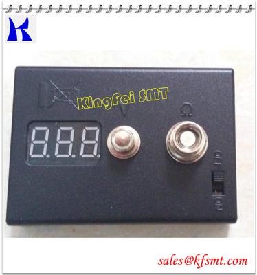
Resistance Tester OHM meter for E Cigarette 510 Thread RDA RBA DIY vaporizer Specifications: Resistance Range: 0-20ω Voltage Range: 0-6V Power Supply: 2 * 1.5V AA Battery(not included) Item Size: 6.7 * 4.6 * 1.6cm / 2.6 * 1.8 * 0.6in Item Weig
Technical Library | 2019-10-16 10:20:25.0
A major goal of the development of advanced packaging technology is to reduce the size, weight, and power consumption of electronics components using state-of-the-art commercial technologies. One of the novel concepts involves the use of all three spatial dimensions when designing and producing new systems. In the past, electronic structures tended to be two dimensional in nature. Generally speaking, individually packaged integrated circuit (IC) dies were interconnected on printed circuit boards. Techniques such as die and package stacking naturally contribute to a reduction of the spatial footprint of any given electronic system design.
Technical Library | 2020-11-09 16:59:53.0
A customer contacted ACI Technologies regarding a high failure rate of their assemblies. They provided assemblies to be X-rayed and inspected for the purpose of identifying any process related issues such as (but not limited to) solder and assembly workmanship and evidence of damage due to moisture related problems during reflow (a.k.a. "popcorning"). Moisture damage usually appears as physical damage to the component. The first indication of moisture damage would be externally observable changes to the package in the form of bulging or fractures to the outer surface of the component, an example of which is shown in Figure 1. Internally observable indicators of moisture damage typically include fractures to the die inside the package and lifted or fractured wire bonds. These conditions would be apparent during transmissive X-ray inspection. Another symptom of moisture related damage would be inconsistent solder joint sizes that result from package deformation during the liquidus phase of the reflow process. None of these indicators of moisture related damage were present on the customer samples.

www.unisoft-cim.com/pcbtest.htm - In minutes the Unisoft ProntoTEST-FIXTURE software translates CAD & BOM files into real reference designators, netlists, X/Y component pin geometries, values, tolerances, part numbers, etc. This data is used by Test
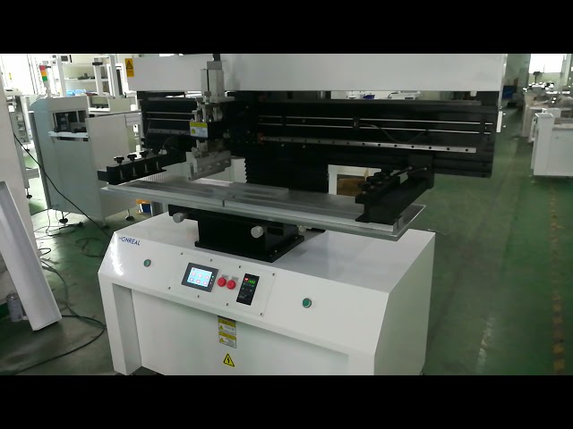
SMT Semi Auto Screen Printer for pcb size 1200 in smt LED production line Product introduction: 1.Using precision guide rail and the import motor to drive the blade seat conversion, printing, and high accuracy. 2.Printing scraper can rotate 45
Training Courses | | | PCB Design Courses
The PCB design courses teach students the process, techniques and tools needed to design layout of printed circuit boards.
Events Calendar | Tue Sep 08 00:00:00 EDT 2020 - Tue Sep 08 00:00:00 EDT 2020 | ,
Post – Moore's Law Electronics: From Now until Quantum Computing
Events Calendar | Mon Apr 23 00:00:00 EDT 2018 - Thu Apr 26 00:00:00 EDT 2018 | Shanghai, China
SMTA China East Conference 2018
Career Center | South Plainfield, New Jersey USA | Engineering
Alpha, a business unit of Alent plc and the global leader in the development, manufacturing and sales of innovative specialty materials used in a wide range of industry segments, including electronics assembly, power electronics, die attach, LED ligh
Career Center | Fremont, California USA | Engineering
Job Description: • Has full ownership of HW design and release including HW specification creation, schematic generation, PCB layout, board bring up, and design verification. • Complete PCB design schematic using Orcad capture. • Complete HW desig
Career Center | Duluth, Georgia USA | Management,Sales/Marketing
Over 20 years of experience selling high tech capital equipment for manufacturing. ��Accomplished in territory management, regional sales management, and key account management ��Proficient at managing several projects, coordinating engineering deve
Career Center | Los Gatos, California | Management,Sales/Marketing
Seasoned sales professional skilled in both direct sales and sales management. Recognized for polished communication, negotiation, and problem-solving skills, Excelled in positions where a combination of direct sales and channel sales force developm
GPD Global | https://www.gpd-global.com/pdf/lead-former/CF9-Doc-Package-901-1-01.pdf
CF9 Documentation Package Documentation Package for CF-9 Taped Radial Component Lead Former PN 901-1-01 CONTENTS of CF-9 Documentation Package Operating Guide In addition to installation, set up, and
Whizz Systems | https://www.whizzsystems.com/ic-package-design/
Electronics IC Package Design Skip to content Electronics IC Package Design Services Services + ENGINEERING SERVICES + FPGA DESIGN SERVICES FPGA DESIGN FEATURES FPGA DEVELOPMENT

.gif)

