Industry Directory | Manufacturer
Manufacturer of flex, rigid-flex, and rigid circuit boards. We offer prototype and production delivery options. We manufacture commercial, military, medical and industrial jobs and offer value added services such as assembly. We can customize services to fit your needs, such as gold or white tin plating, plugged or blind vias, etc.
Industry Directory | Manufacturer
PWB designs and manufactures test equipment and provides services to test the reliability of Printed Circuit Boards.
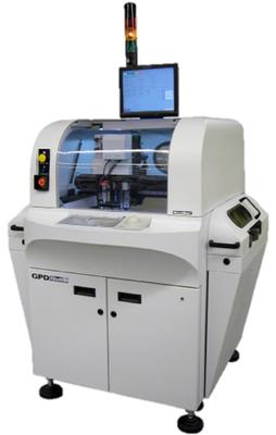
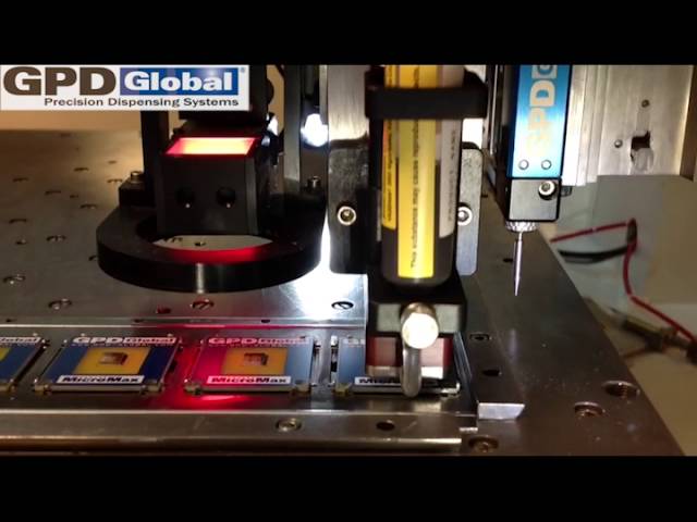
Precision Dispensing System for Heated Dispense Applications The GPD Global MAX II is a compact; high-accuracy system designed for today’s advanced heated dispensing applications. The frame is molded from “liquid rock” which gives the system a stabl
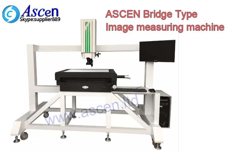
Bridge Type Image measuring machine Instrument features: 1.Adopt high precision grantie structure, never deformation,high stablility and high end good looking . 2.Adopted high-precision optical granite structure ,high resolution color charge-c
Electronics Forum | Sat Aug 28 11:03:44 EDT 2004 | mariels
We are currently designing a multi-layer board using a BGA with a pitch of 1mm. Need to find out what hole/pad size via and if they should be plated holes? Thanks
Electronics Forum | Mon Dec 16 10:54:48 EST 2002 | davef
Knee of barrel and pad crack: Caused by thermal stress during soldering, because epoxy expands in the "z" 3X more than "x" or "y" which are restricted by the fiber. Related to: * Design of pads too large relative to hole diameter * Temperature at o
Used SMT Equipment | AOI / Automated Optical Inspection
11/07/2003 Mirtec MV-2HTL Bench Top AOI inspection machine, as pictured, 110VAC - 240VAC Single phase power per the name plate, buyer needs to confirm any transformer power in wiring - currently set to and powered up with 110VAC power in, Windows O/S
Used SMT Equipment | Coating and Encapsulation
NEW LISTING: PVA Sigma Benchtop Conformal Coating Machine * Facilities Power 120V-220V +/-10%, 50-60 Hz Air 80 psi, dry unlubricated Exhaust 300 cfm * Specifications X-Axis Stroke 330 mm (13.00”) Y-Axis Stroke 300 mm (11.81”) Z-Axis Stroke 100 mm
Industry News | 2010-04-10 02:09:54.0
If a picture is worth a thousand words, the new H revision of IPC-A-600, Acceptability of Printed Boards, is a priceless work of art for fabricators and assemblers, particularly inspectors and product developers. IPC — Association Connecting Electronics Industries® announces the new releases of IPC-A-600H and its companion document the C revision of IPC-6012, Qualification and Performance Specification for Rigid Printed Boards.
Industry News | 2013-01-15 15:44:14.0
, IPC-2221B, Generic Standard on Printed Board Design, provides a basis for the design of all types of printed boards and addresses areas as diverse as testing, via protection, test coupon designs and surface finishes.
Parts & Supplies | Circuit Board Assembly Products
Feeder Parts PCB Board Assembly NEW Condition 40007370 smt feeder parts for juki fx-1 r base-feeder pcb 40007370 copy new Describtion: Part Number: 40007370 Part name: feeder cover condition: copy new Application: JUKI feeder parts : We st

Parts & Supplies | Adhesive Dispensers
Genuine MYDATA parts Brand New; Used( good condition). Available in stock. Quick shipping; Any interesting, feel free to contact via mail: yzfs1968@aliyun.com, Mobile: +86-13501595476 The parts for Mycronic jetting machines(MY500,MY600,
Technical Library | 2019-06-26 23:21:49.0
Copper-filled micro-vias are a key technology in high density interconnect (HDI) designs that have enabled increasing miniaturization and densification of printed circuit boards for the next generation of electronic products. Compared with standard plated through holes (PTHs) copper filled vias provide greater design flexibility, improved signal performance, and can potentially help reduce layer count, thus reducing cost. Considering these advantages, there are strong incentives to optimize the via filling process. This paper presents an innovative DC acid copper via fill formulation, for VCP (Vertical Continues Plating) applications which rapidly fills vias while minimizing surface plating.
Technical Library | 2019-07-17 17:56:34.0
The increased demand for electronic devices in recent years has led to an extensive research in the field to meet the requirements of the industry. Electrolytic copper has been an important technology in the fabrication of PCBs and semiconductors. Aqueous sulfuric acid baths are explored for filling or building up with copper structures like blind micro vias (BMV), trenches, through holes (TH), and pillar bumps. As circuit miniaturization continues, developing a process that simultaneously fills vias and plates TH with various sizes and aspect ratios, while minimizing the surface copper thickness is critical. Filling BMV and plating TH at the same time, presents great difficulties for the PCB manufactures. The conventional copper plating processes that provide good via fill and leveling of the deposit tend to worsen the throwing power (TP) of the electroplating bath. TP is defined as the ratio of the deposit copper thickness in the center of the through hole to its thickness at the surface. In this paper an optimization of recently developed innovative, one step acid copper plating technology for filling vias with a minimal surface thickness and plating through holes is presented.
Precision Dispensing System for Heated Dispense Applications The GPD Global MAX II is a compact; high-accuracy system designed for today’s advanced heated dispensing applications. The frame is molded from “liquid rock” which gives the system a stabl
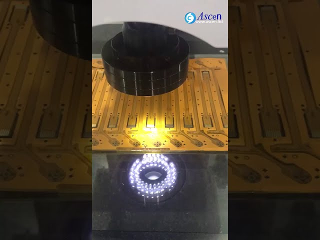
https://www.ascen.ltd/Products/PCB_board_assembly_system/vision_measurin/507.html Vision Measuring Machine and image measuring instrument can be used for dimensional accuracy measurement of various molds, aircraft, automobile, mobile phone, computer,
Training Courses | | | IPC-6012 Specialist (CIS)
The Certified IPC-6012 Specialist (CIS) training covers design, fabrication and inspection of rigid printed boards.
Training Courses | | | IPC-6012 Trainer (CIT)
The Certified IPC-6012 Trainer (CIT) courses recognize individuals as qualified trainers in the area of design, fabrication and inspection of rigid printed boards and prepare them to deliver Certified IPC-6012 Specialist (CIS) training.
Career Center | Dana Point, California USA | Sales/Marketing
We are currently seeking sales reps nationwide for this rapidly growing supplier of printed circuit boards (since 1986)with facilities in southern CA and eight PCB facilities in China and Taiwan, all ISO 9002 certified and UL94V-0 approved, some are
Career Center | , | Engineering,Research and Development,Technical Support
INTRODUCTION Ref: TR/EMP/EXP/VOL.IV/05 Mobil Consulting/Recruiting Services; Pursuant to the service contract with the NIGERIAN MOBIL OIL COMPANY (NMOC) FIELD DEVELOPMENT PROJECT in Nigeria, has been mandated to recruit senior services expatriat
Career Center | Alta Loma, California | Engineering,Quality Control,Research and Development
Rigid and Flexible Printed Circuits Plating and Metal Finishing Operations Six Sigma Work Instruction Documentation Process Development Equipment Selection and Specification New Facility Startup Air, Water and Hazardous Waste Environmental Reporting
Career Center | Erode, Tamilnadu India | Engineering
Professional Summary 3+ years of experience in the PCB CAM engineering Exposure to FRONTLINE GENESIS 2000 Having exposure in UCAM Exposure to Create, Array & Panelize it for manufacturability Experienced in Creating impedance cou
SMTnet Express, June 27, 2019, Subscribers: 32,092, Companies: 10,819, Users: 24,882 Advanced Cu Electroplating Process for Any Layer Via Fill Applications with Thin Surface Copper Credits: MacDermid Inc. Copper-filled micro-vias are a key
SMTnet Express, July 18, 2019, Subscribers: 32,162, Companies: 10,836, Users: 24,951 Via Fill and Through Hole Plating Process with Enhanced TH Microdistribution Credits: MacDermid Inc. The increased demand for electronic devices in recent years
Imagineering, Inc. | https://www.pcbnet.com/blog/making-the-most-of-smaller-components-with-hdi-pcbs/
. To make via-in-pad possible, the PCB fabrication process includes a step to plate the via holes and fill the plated vias with epoxy before the via is then covered up with a plated copper

.gif)

