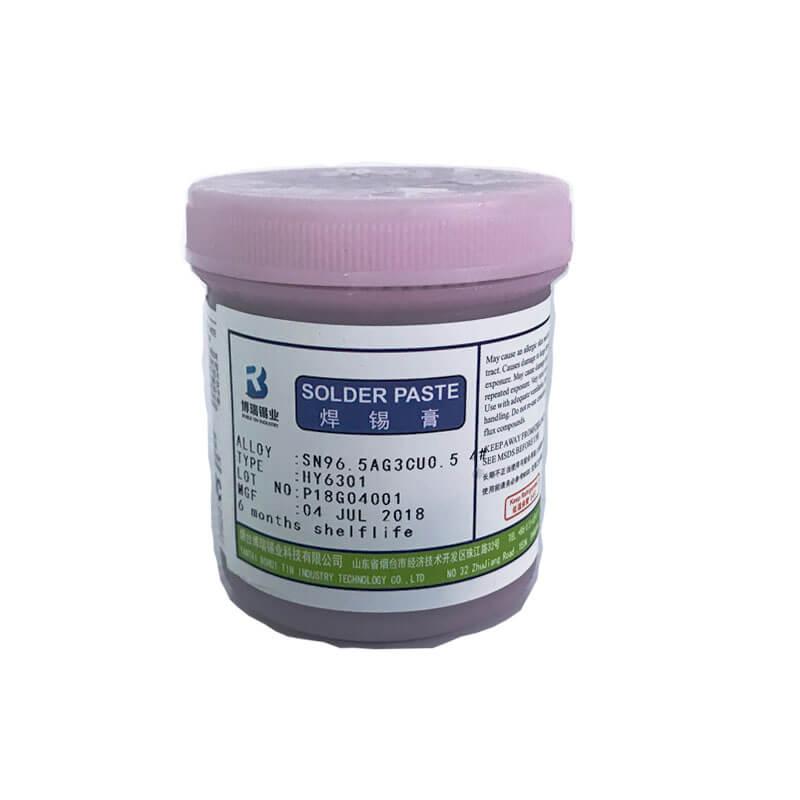
lead-free soldering paste Sn96.5Ag3Cu0.5 lead-free soldering paste Sn96.5Ag3Cu0.5 tin solder paste flux solder paste Product description: lead-free soldering paste Sn96.5Ag3Cu0.5 INQUIRY lead-free soldering paste Sn96.5Ag3Cu0.5 P
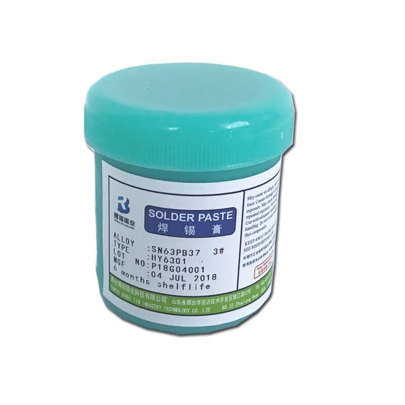
solder paste Sn63/Pb37 solder paste Sn63/Pb37 Tin solder paste Sn63/Pb37 Tin solder paste Sn63/Pb37 Product description: solder paste Sn63/Pb37 INQUIRY solder paste Sn63/Pb37 Specifications: Brands Flason
Electronics Forum | Tue Jul 30 12:15:15 EDT 2002 | Rick Lathrop
Hi Dave, The paste applied to the board ends up on the tombstone. The pad has a thin covering of solder most of the time, this is why I think they call it a dewet. Occasionally the pad shows some areas of gold and very rarely are some pads not wet at
Electronics Forum | Tue May 13 08:26:29 EDT 2008 | davef
First, on your reflow temperature comment: The 183*C focus for reflow recipes for tin-lead solder is a falicy. If you held a recipe for tin-lead solder at 183*C peak, it would never reflow. Recipes for tin-lead solder need to be at liquidus plus 20*C
Industry News | 2018-12-08 03:29:29.0
SMT Dictionary – Surface Mount Technology Acronym and Abbreviation
Technical Library | 2023-08-04 15:27:30.0
A designed experiment evaluated the influence of several variables on appearance and strength of Pb-free solder joints. Components, with leads finished with nickel-palladium-gold (NiPdAu), were used from Texas Instruments (TI) and two other integrated circuit suppliers. Pb-free solder paste used was tin-silver-copper (SnAgCu) alloy. Variables were printed wiring board (PWB) pad size/stencil aperture (the pad finish was consistent; electrolysis Ni/immersion Au), reflow atmosphere, reflow temperature, Pd thickness in the NiPdAu finish, and thermal aging. Height of solder wetting to component lead sides was measured for both ceramic plate and PWB soldering. A third response was solder joint strength; a "lead pull" test determined the maximum force needed to pull the component lead from the PWB. This paper presents a statistical analysis of the designed experiment. Reflow atmosphere and pad size/stencil aperture have the greatest contribution to the height of lead side wetting. Reflow temperature, palladium thickness, and preconditioning had very little impact on side-wetting height. For lead pull, variance in the data was relatively small and the factors tested had little impact.
Technical Library | 2024-04-08 15:46:36.0
A designed experiment evaluated the influence of several variables on appearance and strength of Pb-free solder joints. Components, with leads finished with nickel-palladium-gold (NiPdAu), were used from Texas Instruments (TI) and two other integrated circuit suppliers. Pb-free solder paste used was tin-silver-copper (SnAgCu) alloy. Variables were printed wiring board (PWB) pad size/stencil aperture (the pad finish was consistent; electrolysis Ni/immersion Au), reflow atmosphere, reflow temperature, Pd thickness in the NiPdAu finish, and thermal aging. Height of solder wetting to component lead sides was measured for both ceramic plate and PWB soldering. A third response was solder joint strength; a "lead pull" test determined the maximum force needed to pull the component lead from the PWB. This paper presents a statistical analysis of the designed experiment. Reflow atmosphere and pad size/stencil aperture have the greatest contribution to the height of lead side wetting. Reflow temperature, palladium thickness, and preconditioning had very little impact on side-wetting height. For lead pull, variance in the data was relatively small and the factors tested had little impact.
ATTENDANT WET CHEMICAL PROCESSES) Hole wall preparatio
PCB Libraries, Inc. | https://www.pcblibraries.com/forum/topic995&OB=ASC.html
. Now we have the problem of poor wetting. The wave soldering diection is correct. My question is also is there difference between reflow soldering footprint and the wave soldering footprint
Blackfox Training Institute, LLC | https://www.blackfox.com/4-common-errors-in-smt-assembly/
. Non Wetting Or De Wetting Non-wetting is an SMT defect that occurs when the base metal surface on the board doesn’t accept the molten solder, creating a poor joint condition where a component’s terminals

COT specializes in high quality SMT nozzles and consumables for pick and place machines. We provide special engineering design service of custom nozzles for those unique and odd components.
2481 Hilton Drive
Gainesville, GA USA
Phone: (770) 538-0411


