Industry Directory | Distributor / Manufacturer / Manufacturer's Representative / Standards Setting / Certification / Training Provider
PB Technik supplies SMT equipment and materials to the Polish market. JUKI ERSA EKRA BRADY MARANTZ

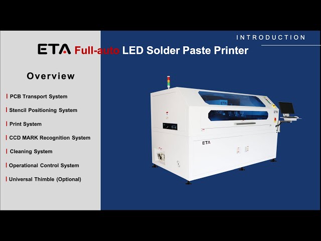
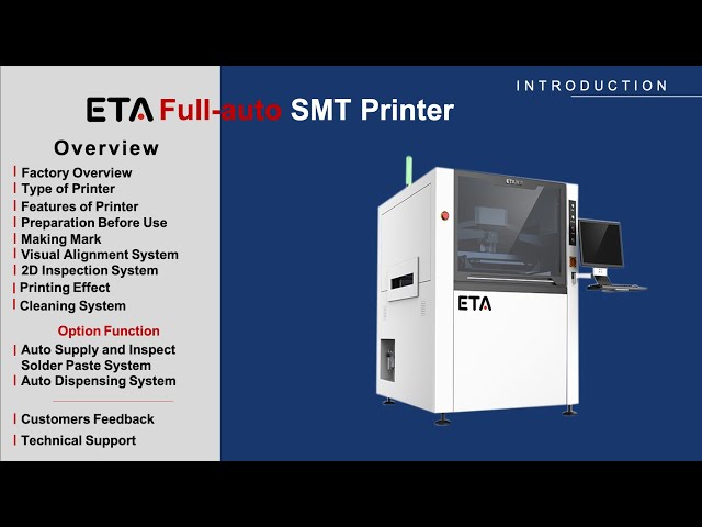
ETA NEW Fully Auto SMT Stencil Screen Printer for LED ❙ Introduce of SMT Printer ETA ETA-4034 is a high precision automatic solder paste printer, correspond to industrial 4.0 and MES system.through a higher level of automation, ac
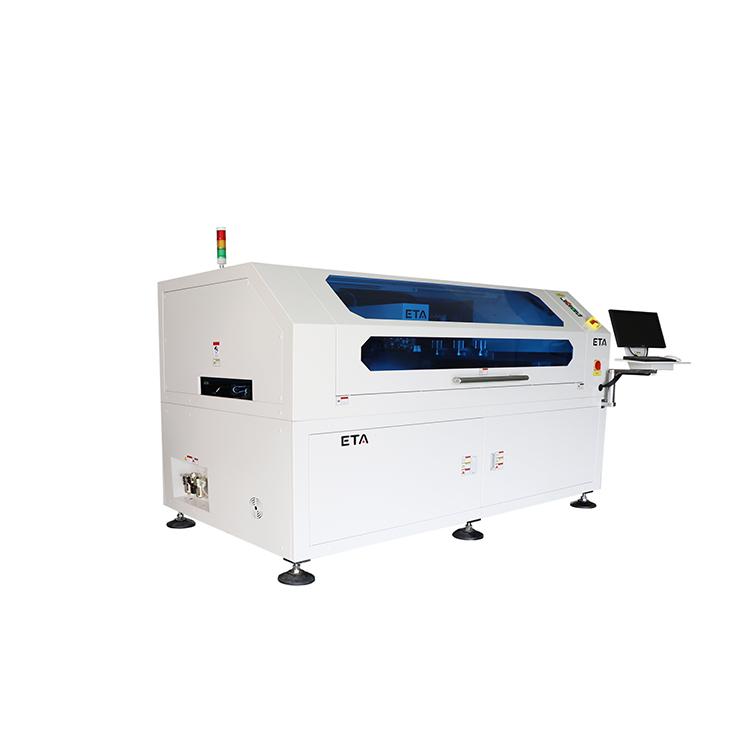
Good Service SMT Stencil Printer for PCB Assembly Line ❙ Introduce of SMT Printer ETA ETA-4034 is a high precision automatic solder paste printer, correspond to industrial 4.0 and MES system.through a higher level of automa
Electronics Forum | Thu Sep 02 21:02:55 EDT 1999 | Paul Wareham
We've noticed that there are many different recommendations for pad sizes for various SMT parts. This seems to vary wildly from manufacturer to manufacturer for the same case sizes. Is there any standards that can used used to specify these sizes?
Electronics Forum | Wed May 09 10:40:10 EDT 2001 | davef
First, your primary side component pads should be designed according to SM-782A, "Surface Mount design & Land Pattern Standard". Next if you did that and your secondary side component pads are the same size as your primary side components, your diff
Industry News | 2019-11-05 22:07:01.0
Tenting a via refers to covering via with soldermask to enclose or skin over the opening. A via is a hole drilled into the PCB that allows multiple layers on the PCB to be connected to each other. A non tented via is just a via that is not covered with the soldermask layer. Leaving these vias exposed or covered has pros and cons depending on the your design and manufacturing requirements.
Industry News | 2018-10-18 11:19:07.0
How To Design Cost-Effective PCBs
ETA NEW Fully Auto SMT Stencil Screen Printer for LED ❙ Introduce of SMT Printer ETA ETA-4034 is a high precision automatic solder paste printer, correspond to industrial 4.0 and MES system.through a higher level of automation, ac
Good Service SMT Stencil Printer for PCB Assembly Line ❙ Introduce of SMT Printer ETA ETA-4034 is a high precision automatic solder paste printer, correspond to industrial 4.0 and MES system.through a higher level of automa
| https://www.smtfactory.com/Hot-Air-8-Trays-Electric-Reflow-Convection-Oven-with-High-Quality-pd48530624.html
Reflow Wave Oven Reflow Oven Smd Smt Reflow Soldering Oven Reflow Oven Heating Reflow Oven Mini Smt Reflow Oven Reflow Oven Nitrogen Reflow Oven Desktop Reflow Oven Heating Element Reflow Oven
| http://etasmt.com/te_news_bulletin/2021-08-31/23567.chtml
. Subsequent experiences by the author with users is consistent with this figure. The initial design of the board, particularly pad geometries and solder mask parameters, also have a profound effect on the quality of soldering accomplished


