Industry Directory | Manufacturer
We manufacture laser stencil for the PCB industry.
Industry Directory | Consultant / Service Provider / Manufacturer / Other
Located in Oradea, Romania, NDS is a manufacturer of laser cut stencils for SMT. We are offering stencils for Romanian and worldwide market at the best quality-price ratio.
New Equipment | Solder Paste Stencils
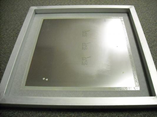
SMT Framed Stencils are laser cut solder paste stencils designed to work on SMT printing machines. These laser cut stencils are permanently glued into a frame. These framed stencils are are designed for highly repeatable continuous operation in volum
New Equipment | Solder Paste Stencils
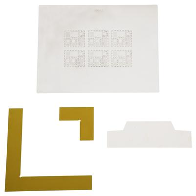
SMT Foil Stencils are laser cut solder paste stencils designed to work on their own for hand printing or with stencil tensioning systems. These laser cut stencils do not need to be permanently glued in a frame. These so-called frameless stencils are
Electronics Forum | Tue Sep 22 10:05:00 EDT 2009 | roland_grenier
Does anyone know how to calculate solder paste volume required to run a PCBA on an SMT line? I'm looking for a solder paste volume model which include paste waste. Roland
Electronics Forum | Thu Jun 01 05:06:10 EDT 2006 | EC
Hi, I facing some 1005 component with poor wetting and look like not enough solder...... Is there any standard solder paste volume requirement. Appreciate all the input.

Used SMT Equipment | AOI / Automated Optical Inspection
Board dimensions: 3 in. to 18 in. Configuration: * includes repair PC w/ repair s/w * s/w upgraded in 2013 - version 5.4 build 2013053 Camera: 3D Wide IVP / Pulnix 2048 x 2040 Software key: * PTH Post Solder * SMT Post Solder * Paste: Volum
Used SMT Equipment | SPI / Solder Paste Inspection
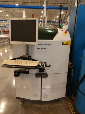
Agilent SP50 Series II 3D SPI 3D Solder Paste Inspection System Model: SP50 Series II Vintage: 2006 Maximum board size: 510 by 510 mm (20 by 20 in) Minimum board size: 50 by 50 mm (1.97 by 1.97 in) Maximum board thickness: 4 mm (0.16 in) 2D an
Industry News | 2017-07-23 20:13:17.0
SMTA announces an expanded program for the final day of the SMTA International Conference, September 17 - 21, 2017 in Rosemont, Illinois. In addition to the Lead-Free Symposium, the technical committee expanded the Thursday program to four concurrent tracks. The three additional tracks will focus on Advanced Packaging Technology, Manufacturing Excellence, and Inspection Technologies.
Industry News | 2012-10-16 18:56:39.0
IPC — Association Connecting Electronics Industries® will hold “IPC Conference on Solderability and Reliability for Electronics Assemblies” on 6-7 February 2013, in Budapest, Hungary.
Technical Library | 2019-05-29 23:10:30.0
There are times when a PCB prototype needs to be built quickly to test out a design. In such cases where it is known early on that there will be multiple iterations or that a "one and done" assembly will be made that there will be some SMT assemblers who choose to hand print solder paste onto the board using a "frameless" stencil. In such cases where hand printing is used, the consistency of the printing technique has typically been in question. Furthermore, the effectiveness of both the nanocoatings as well as the higher end stainless steel materials, which have been heretofore studied in controlled printing environments, will be evaluated for their impact on the hand printing process.The purpose of the study was to determine the effectiveness of select nanocoating materials as well as certain high end stainless steel stencil materials as they relate to the manual SMT printing process. A variety of nanocoatings were applied to SMT metal stencils and solder paste volume measurements were taken to compare the effectiveness.
Technical Library | 2015-08-25 13:51:27.0
The stencil printing process is one of the most critical processes in the electronic production. Due to the requirement: "faster and smaller" it is necessary to place components with different paste volume close together without regard to solder paste printing. In our days it is no longer possible to control the solder paste volume only by adjustment of the aperture dimensions. The requirements of solder paste volumes for specific components are realized by different thicknesses of metal sheets in one stencil with so called step stencils. The step-down stencil is required when it is desirable to print fine-pitch devices using a thinner stencil foil, but print other devices using a thicker stencil foil. The paper presents the innovative technology of step-up and step-down stencils in a laser cutting and laser welding process. The step-up/step-down stencil is a special development for the adjustment of solder paste quantity, fulfilling the needs of placement and soldering. This includes the laser cutting and laser welding process as well as the resulting stencil characteristics and the potential of the printing process.
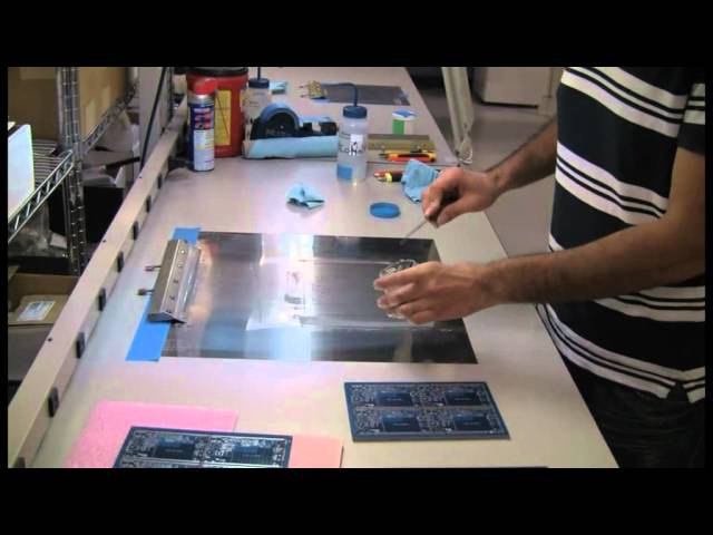
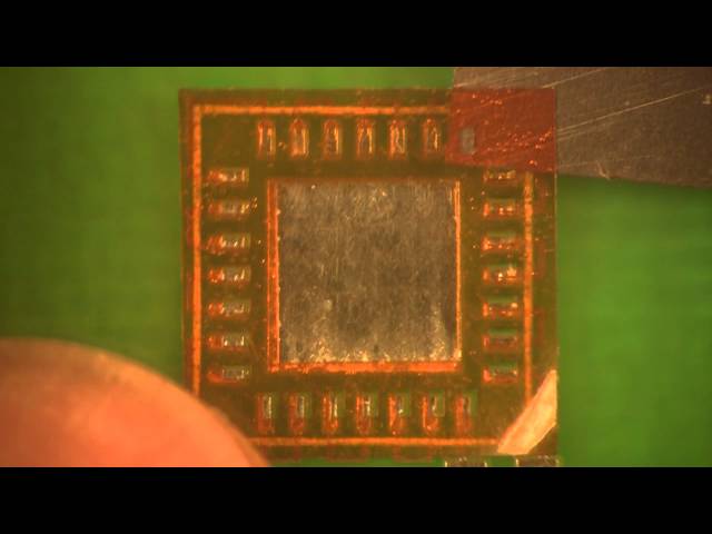
This is video shows how to print a PCB using a prototype foil only stencil. The SMT prototype stencil (www.soldertools.net) is made from a high nickel content material able to offer repeatable high precision apertures. The steps of alignment, printin
Training Courses | | | PCB Assembly Courses
The PCB assembly courses provide knowledge of different processes and equipment used in TH and SMT assembly of printed circuit boards.
Career Center | Rochester, New York USA | Engineering
I have done my undergraduate studies in Mechanical Engineering. I am pursuing my Master's Program in Electronics Packaging. I am currently working as a Research Assistant for RIT-CEMA (Center for Electronics Manufacturing and Assembly). My research
1st Place Machinery Inc. | http://www.firstplacemachinery.com/first_place_smt_pcb_aoi_cyberoptics.html
Cyberoptics Solder Paste Cyberoptics Solder Paste Inspection Model Number: SE200 2D/3D Solder Paste Inspection 115 volt Serial Number: 45026 Year: July 2000 Includes Monitor - Keyboard - Mouse No Manual
| https://pcbasupplies.com/lead-free-solder-paste/
Lead-Free Solder Paste -SAC305 Jet Dispensable Solder Paste - PCBASupplies Login Create Account Contact View My Cart Menu × Categories Hand Soldering


