Industry Directory | Manufacturer
Reflow ovens for automated SMT PCB assembly, specializing in lead free processing and nitrogen reflow. The best convection reflow ovens on the market.

Industry Directory | Manufacturer
A US manufacturer of quality hand tools for those engaged in the repair, rework, R & D, testing, and assembly of electronic components and printed circuit boards from Through Hole to 2Mil Pitch Surface Mount.
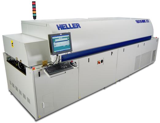
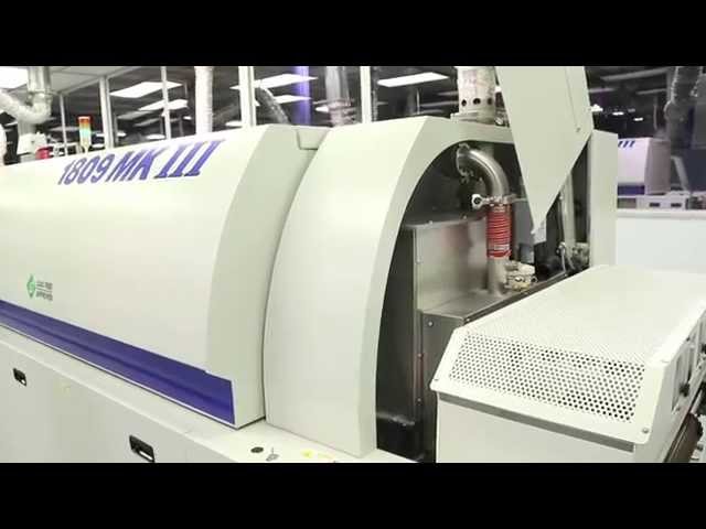
1809 MK5 - Heller Advanced In-Line Vacuum Reflow Oven Nitrogen System with Balanced Flow Technology 9 Top And Bottom Heated Zones - highest zone count per linear foot in the industry! 100" Heated Length - for super throughput! 2 Internal C

Flux Free Formic Reflow Reflow in Formic Acid Vapor Heller has designed and built an production ready horizontal reflow oven for formic acid vapor. This new oven has been designed to meet Semi S2/S8 safety standards (including toxic gases). Form
Electronics Forum | Tue Mar 01 11:19:47 EST 2011 | jeddmartens
I have no knowledge into PCB designing with surface mount components, all my experience has been with through hole components. I now have to design PCBs using surface mount parts. I have a few questions I was hoping someone could answer. Can a PCB w
Electronics Forum | Wed Mar 08 10:52:27 EST 2000 | Wolfgang Busko
Hi Jacqueline, for the "manufacturing allowance" IPC says FAB.TOL. is the board manufacturing tolerance and PLACE ACRCY is the pick and place accuracy. For 0,8 mm pitch they give for both values 0,1 mm. Solder joint design goal data comes from empir
Used SMT Equipment | Soldering - Reflow
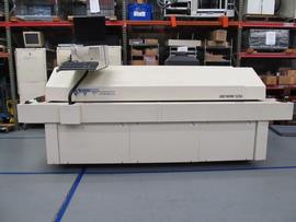
1996 Vitronics Unitherm 520A Reflow Oven Features: 5 Heat Zones Top and Bottom / 2 Cool Zones o Edge and Mesh o Set up for Air - Nitrogen Capable o 220v 3 phase 105 amp o 12’ x 5’ Footprint
Used SMT Equipment | Screen Printers
DEK Horizon 03i automatic stencil printer Specification : DEK Horizon 03i High Precision Automatic Solder Paste Printer designed for high precision steel mesh printing or stencil printing in SMT industry. Printing PCB size: 50x50mm to 508x510mm;
Industry News | 2016-06-22 15:33:28.0
Based on its recent analysis of the surface mount technology (SMT) reflow soldering equipment market, Frost & Sullivan recognizes Heller Industries, Inc. with the 2016 Global Frost & Sullivan Award for Growth Excellence Leadership. Heller Industries has made remarkable improvements to its product and technology portfolios over the last 10 years to emerge a top participant in the SMT reflow soldering equipment market.
Industry News | 2017-09-16 02:29:39.0
Heller Industries has been awarded the 2017 Global Frost & Sullivan Company of the Year Award for its surface mount technology (SMT) soldering equipment that enables Industry 4.0. - the automation and data exchange in manufacturing technologies.
 – pn 51305433.jpg)
Parts & Supplies | Pick and Place/Feeders
0402 Ceramic Blade Nozzle (3030) – p/n 51305433 You might ask, “What’s the difference between this nozzle and the older conical 0402 ceramic nozzle?” Simply put, we think this latest design is a far superior option. Here&
 51305434_1.jpg)
Parts & Supplies | Pick and Place/Feeders
0603 Ceramic Blade Nozzle 3040 51305434 We were so impressed with the new long-life ceramic 0402 nozzle (#3030) we launched earlier in 2014 that we decided to follow it up with an 0603 version! Now customers can reap the benefits of our ESD-Safe ce
Technical Library | 2023-01-17 17:12:33.0
Reflowed indium metal has for decades been the standard for solder thermal interface materials (solder TIMs or sTIMs) in most high-performance computing (HPC) TIM1 applications. The IEEE Heterogeneous Integration Thermal roadmap states that new thermal interface materials solutions must provide a path to the successful application of increased total-package die areas up to 100cm2. While GPU architectures are relatively isothermal during usage, CPU hotspots in complex heterogeneously-integrated modules will need to be able to handle heat flux hotspots up to 1000W/cm2 within the next two years. Indium and its alloys are used as reflowed solder thermal interface materials in both CPU and GPU "die to lid/heat spreader" (TIM1) applications. Their high bulk thermal conductivity and proven long-term reliability suit them well for extreme thermomechanical stresses. Voiding is the most important failure mode and has been studied by x-ray. The effects of surface pretreatment, pressure during reflow, solder flux type/fluxless processing, and preform design parameters, such as alloy type, are also examined. The paper includes data on both vacuum and pressure (autoclave) reflow of sTIMs, which is becoming necessary to meet upcoming requirements for ultralow voiding in some instances.
Technical Library | 2021-01-03 19:24:52.0
Reflow soldering is the primary method for interconnecting surface mount technology (SMT) applications. Successful implementation of this process depends on whether a low defect rate can be achieved. In general, defects often can be attributed to causes rooted in all three aspects, including materials, processes, and designs. Troubleshooting of reflow soldering requires identification and elimination of root causes. Where correcting these causes may be beyond the reach of manufacturers, further optimizing the other relevant factors becomes the next best option in order to minimize the defect rate.
Nano-copper sintering in formic acid vapor.
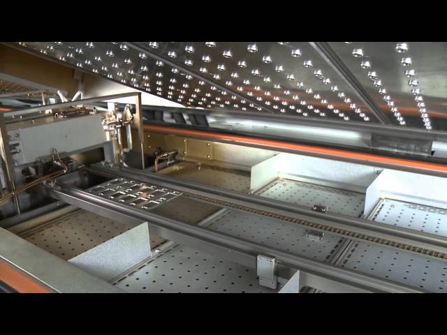
1809 MK5 - Heller Advanced In-Line Vacuum Reflow Oven Nitrogen System with Balanced Flow Technology 9 Top And Bottom Heated Zones - highest zone count per linear foot in the industry! 100" Heated Length - for super throughput! 2 Internal C
Training Courses | | | PCB Rework and Hand Soldering Courses
The PCB rework and hand soldering courses courses cover techniques of rework and repair of PCBs, BGAs and other electronics assemblies, and teach fundamentals of soldering of electronics assemblies.
Training Courses | | | IPC-600 Specialist (CIS)
The Certified IPC-600 Specialist (CIS) training targets quality assurance and acceptance of bare printed circuit boards.
Events Calendar | Thu Mar 18 00:00:00 EDT 2021 - Thu Mar 18 00:00:00 EDT 2021 | ,
India Chapter Webinar: PCBA Process Qualifications
Events Calendar | Mon Dec 02 00:00:00 EST 2019 - Mon Dec 02 00:00:00 EST 2019 | ,
Webinar: QFN/LGA Design, Assembly Process Issues & Reliability Failures
Career Center | San Jose, CA, California USA | Engineering,Production,Research and Development
Senior PCB Designer: Want to be part of an exciting pre-IPO enterprise B2B company working on the cutting edge of internet-of-things, artificial intelligence & agents, blockchain, and manufacturing technology? This well-funded venture-backed co
Career Center | Space Coast, Florida USA | Engineering,Research and Development
Board Level Assembly BGA Expert! We are in need of an Electronic Packaging or Advanced Manufacturing Engineer to work with the Advanced Manufacturing Technology Group of a major Florida based Communications company. Support IR&D and Program activit
Career Center | Colton, California USA | Engineering,Maintenance,Production,Quality Control,Research and Development,Technical Support
• Strong experience with the installation, training, and repair on a variety of electro-mechanical, pneumatic, PLC, or computer controlled systems. • Strong Knowledge in SMT equipment, Screen Printer, AOI/SPI, Conformal Coat Systems, Reflow oven, X-R
Career Center | Newport Beach, California USA | Engineering,Management,Production
KEVIN RAGER P.O.BOX 7878, NEWPORT BEACH, 949 922 8997, KEVIN.RAGER@EDA-INC.US OBJECTIVE I am trying to find a consistent work flow that provides mentally challenging yet stimulating experiences in design and prototype development. EXPERIENCE 1997
SMTnet Express, September 27, 2018, Subscribers: 31,354, Companies: 11,055, Users: 25,237 Assessing the Effectiveness of I/O Stencil Aperture Modifications on BTC Void Reduction Carlos Tafoya, Gustavo Ramirez, Timothy O'Neill; AIM Solder Bottom
ASYMTEK Products | Nordson Electronics Solutions | https://www.nordson.com/en/our-company/corporate-responsibility/environmental-footprint
. In turn, these practices also lower our carbon footprint. Additionally, as we design products and manufacturing processes, we seek opportunities to reduce our products
Whizz Systems | https://www.whizzsystems.com/wp-content/uploads/2021/09/5G-design-reference-platform.pdf
5G Reference Design Platform 5G -NR Open-Radio Unit (O-RU) Reference Design Platform Get your radio design up and running quickly with reference design enablement The Radio Access Network (RAN


