Industry Directory | Manufacturer
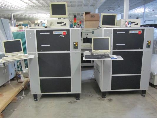
Selective Soldering Equipment and Solutions for Printed Circuit Board Assembly
Industry Directory | Manufacturer
Shuttle Star Technology designs and builds advanced off-line 2.5D&3D x-ray inspection systems for solder joint and final assembly test inspection in SMT&EMS. It uses world-class X-ray techniques with advanced defect detection.

High precision smt aoi offline machine pcba offline aoi 2 conveyor aoi Technical parameter: ategory project specifications Visual identity system Discrimin

The PCB Footprint Expert is a powerful CAD library development tool powered by our own proprietary CAD LEAP Technology (Libraries Enhanced with Automated Preferences). It is packed with very powerful advanced library management features that cuts foo
Electronics Forum | Fri Jan 12 15:50:51 EST 2007 | pyro747
Hello all, We have resently run across a solder joint from a through hole part that looks to have a wrinkle effect (star look) from the wave? No pattern it just happens here and there, and some of the joints on the same row look smooth and good. Any
Electronics Forum | Thu Nov 20 16:51:48 EST 2014 | joe98375
gregp: Our PTH process has not changed in many years. Our products are fairly simple as far as electronics goes and everything gets potted anyways. ~90% of everything we build is single sided TH with ~ 100 solder joints per board. Each board is ~
Used SMT Equipment | AOI / Automated Optical Inspection
(2) Orbotech Automated Optical Inspections Machines For Sale Machine were just taken out of Military OEM facility in good working condition Both machines are being sold together at discounted price See attached pictures and information below
Industry News | 2016-08-25 17:56:34.0
GPD Global's advanced Precision Auger Pump retrofits into your dispensing system to provide excellent dispense control and repeatability. Precision Auger Pump Integration provides your process development with a broad range of functionality.
Industry News | 2011-11-03 21:52:00.0
By davef: I was fortunate to be able to attend the SMTAI Exhibition Oct. 18-19, 2011. While I was walking around looking at the booths and talking to the exhibitors, I got this idea that I would report back on things that I found interesting. You know spread the news, since not everyone was there.

Parts & Supplies | SPI / Solder Paste Inspection
Quick programming, friendly programming interface Multiple measurement methods True one-button measurement Eight-way motion button, one-click focus Adjustable scanning pitch Solder paste 3D simulation function Powerful SPC function MARK
Technical Library | 2019-06-21 10:39:15.0
Recently, an ACI Technologies (ACI) customer called to discuss failures that they had observed with some through-hole capacitor parts. The components were experiencing failures following vibration and accelerated stress testing. Upon receipt of the samples, ACI performed three levels of inspection and Energy Dispersive Spectroscopy (EDS) testing to investigate the root cause of the failures. These analyses enabled ACI to verify the elements comprising the solder joints and make the following recommendations in order to prevent future occurrences. The first inspection was to investigate the capacitor leads using optical microscopy, and no anomalies were found that could indicate bad parts from the vendor or improper handling prior to assembly. However, vertical fill in the barrel of the plated through-holes was too close to the IPC-A-610 minimum specification of 75% to determine a pass/fail condition, and therefore required further investigation.
Technical Library | 2019-10-10 00:26:28.0
Voids are a plague to our electronics and must be eliminated! Over the last few years we have studied voiding in solder joints and published three technical papers on methods to "Fill the Void." This paper is part four of this series. The focus of this work is to mitigate voids for via in pad circuit board designs. Via holes in Quad Flat No-Lead (QFN) thermal pads create voiding issues. Gasses can come out of via holes and rise into the solder joint creating voids. Solder can also flow down into the via holes creating gaps in the solder joint. One method of preventing this is via plugging. Via holes can be plugged, capped, or left open. These via plugging options were compared and contrasted to each other with respect to voiding. Another method of minimizing voiding is through solder paste stencil design. Solder paste can be printed around the via holes with gas escape routes. This prevents gasses from via holes from being trapped in the solder joint. Several stencil designs were tested and voiding performance compared and contrasted. In many cases voiding will be reduced only if a combination of mitigation strategies are used. Recommendations for combinations of via hole plugging and stencil design are given. The aim of this paper is to help the reader to "Fill the Void."
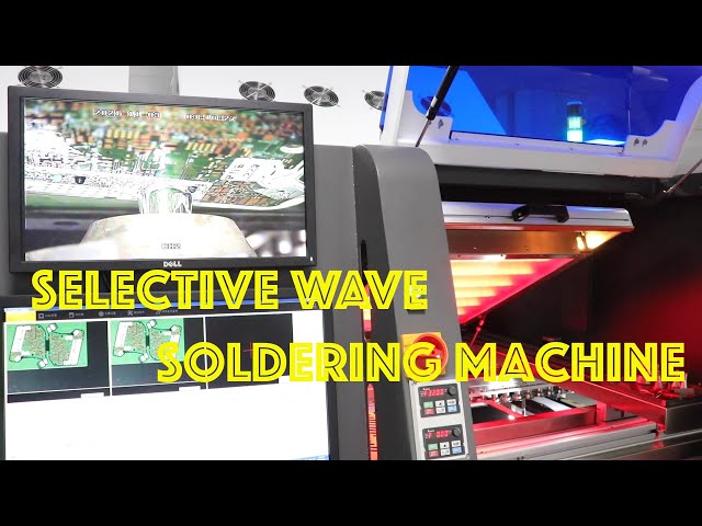
Wave soldering is the standard process that has been in use for many years to solder parts onto a circuit board. ... Selective soldering is an automated system that pumps molten solder up from a reservoir through a nozzle to coat the leads extending

The PCB Footprint Expert is a powerful CAD library development tool powered by our own proprietary CAD LEAP Technology (Libraries Enhanced with Automated Preferences). It is packed with very powerful advanced library management features that cuts foo
Training Courses | | | PCB Rework and Hand Soldering Courses
The PCB rework and hand soldering courses courses cover techniques of rework and repair of PCBs, BGAs and other electronics assemblies, and teach fundamentals of soldering of electronics assemblies.
Training Courses | | | PCB Rework and Hand Soldering Courses
The PCB rework and hand soldering courses courses cover techniques of rework and repair of PCBs, BGAs and other electronics assemblies, and teach fundamentals of soldering of electronics assemblies.
Events Calendar | Thu Oct 21 00:00:00 EDT 2021 - Thu Oct 21 00:00:00 EDT 2021 | ,
Great Lakes Chapter Webinar: Low Melting Alloy & Selection of the Right Chemistry for Reliability
Career Center | Danville, Illinois USA | Production
http://jobs-watchfiresigns.icims.com/watchfiresigns_jobs/jobs/candidate/job.jsp?jobid=1005&mode=view Overview: Watchfire Signs is a dynamic, exciting place to work. Our process engineers utilize their required Bachelors of Engineering and required
Career Center | Melbourne, Florida USA | Production
The SMD Repair / Operator performs all hand loading/unloading/operation of SMD line, manual soldering of Through-hole parts, inspection of PCBA's, and rework as required to support SMD production. Responsibilities: - Assists with manually load
Career Center | Princeton, Texas USA | Production,Quality Control
I have years of experinece in the electronics field which include: component verification, prepping thru hole parts, building pc boards, soldering thru-hole and smt boards, QA etc.
Career Center | Gurgaon, Haryana India | Management
� Heading daily morning meeting with all program managers, materials manager, test engineering manager, process engineering manager, quality control manager, planning manager, stock room manager, shipping department head. Discussion about incoming or
INSERT INTO tracking_express (userid, username, page_id, ts) VALUES ('#Quser_profile.id#', '#Quser_profile.username#', 9, (#ts#)) SMT Express, Volume 2, Issue No. 1 - from SMTnet.com Volume 2, Issue No. 1 Thursday, January 20, 2000
SMT Express, Volume 2, Issue No. 3 - from SMTnet.com Volume 2, Issue No. 3 Thursday, March 16, 2000 Featured Article Return to Front Page Stencil Design for Mixed Technology Through-hole / SMT Placement and Reflow by William E. Coleman, Photo
ASCEN Technology | https://www.ascen.ltd/Products/insertion_feeder/926.html
Through hole part insertion feeder-PCB magazine loader,PCB turn conveyor,pcb conformal coating machine,PCB router,PCB depaneling machine,pcb buffer conveyor from ASCEN technology Welcome to visit ASCEN | | | | | | | Cart
PCB Libraries, Inc. | https://www.pcblibraries.com/forum/jstd001-plated-throughhole-obstruction_topic2145_post9247.html
. To avoid Hole Obstruction, component manufacturers are forming the package body to lift it off the PCB allowing the Air in the hole to be pushed out and form an adequate solder joint


