New Equipment | Assembly Services
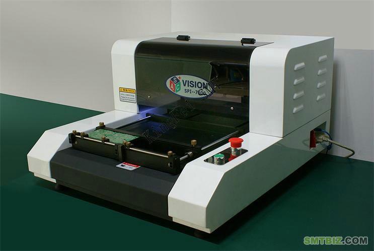
Detailed introduction of 3D spi-7500 solder paste thickness gauge Product function Fast programming, friendly programming interface 1. Multiple measurement methods 2. True one button measurement 3. Eight square movement button, one key foc
New Equipment | Assembly Services
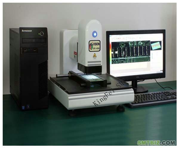
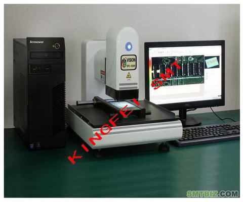
Detailed introduction of 3D spi-6500 solder paste thickness gauge Product function 1. Friendly programming interface 2. Multiple measurement methods 3. The scanning distance is adjustable 4. 3D simulation function of image 5. Independent
Electronics Forum | Tue Jan 07 23:38:08 EST 2014 | m_imtiaz
want to know the tolerance the paste height in the solder paste printing. for example if stencil thickness is 7 mil, what will the acceptance level of paste height ( upper and lower) kindly share if any guidelines or formula for the same
Electronics Forum | Fri Jan 24 08:14:24 EST 2014 | davem
m_imtiaz, Over the last 15 years or so I've found that using the stencil foil thickness +2mils/-0mils has worked very well. For example, if you have a 5mil stencil thickness your upper control limit would be 7mils and your lower control limit would
Used SMT Equipment | Pick and Place/Feeders
Product Details of 3D SPI-6500 Thick Paste Measurement Instrument Product Functions 1, friendly programming interface 2, a variety of measurement methods 3, scan spacing adjustable 4, image 3D simulation function 5, independent 3D dynamic obser
Used SMT Equipment | AOI / Automated Optical Inspection
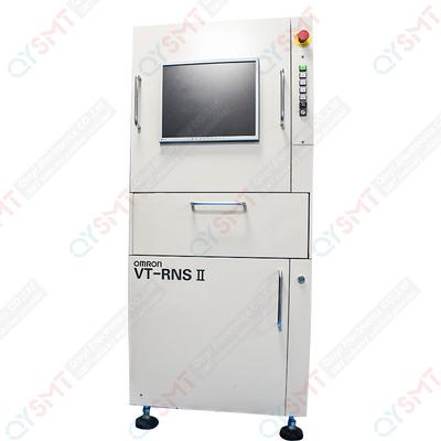
OMRON AOI VT-RNS2-L Omron AoiVT-RNSⅡ parameters Hardware part LSIZE Image signal input part Camera 3CCD camera Lighting series Ring LED (R.G.B) Image resolution 10, 15, 20um Mechanism part Transmission method Belt transmission method Producti
Industry News | 2023-10-16 12:50:01.0
MIRTEC announces the release of their All-New ART Hybrid 3D AOI System at Productronica 2023. The World's leading trade fair for the electronics manufacturing industry will take place Nov. 14-17, 2023, at the Trade Fair Center Messe München, Germany. All are welcome to MIRTEC's Booth #461 in Hall A2 for a detailed demonstration of what will undoubtedly be recognized as the World's Most Technologically Advanced 3D AOI System!
Industry News | 2011-03-14 17:53:00.0
Christopher Associates announces that Jasbir Bath, Consulting Engineer, will Chair the session titled "Reflow Assembly" at the upcoming IPC APEX EXPO, scheduled to take place April 12-14, 2011 at the Mandalay Bay Resort & Convention Center in Las Vegas. The session will take place Tuesday, April 12, 2011 from 1:30-3 p.m.

Parts & Supplies | SPI / Solder Paste Inspection
Quick programming, friendly programming interface Multiple measurement methods True one-button measurement Eight-way motion button, one-click focus Adjustable scanning pitch Solder paste 3D simulation function Powerful SPC function MARK
Technical Library | 2023-07-25 16:50:02.0
Some of the new handheld communication devices offer real challenges to the paste printing process. Normally, there are very small devices like 01005 chip components as well as 0.3 mm pitch uBGA along with other devices that require higher deposits of solder paste. Surface mount connectors or RF shields with coplanarity issues fall into this category. Aperture sizes for the small devices require a stencil thickness in the 50 to 75 um (2-3 mils) range for effective paste transfer whereas the RF shield and SMT connector would like at least 150 um (6 mils) paste height. Spacing is too small to use normal step stencils. This paper will explore a different type of step stencil for this application; a "Two-Print Stencil Process" step stencil. Here is a brief description of a "Two-Print Stencil Process". A 50 to 75 um (2-3 mils) stencil is used to print solder paste for the 01005, 0.3 mm pitch uBGA and other fine pitch components. While this paste is still wet a second in-line stencil printer is used to print all other components using a second thicker stencil. This second stencil has relief pockets on the contact side of the stencil any paste was printed with the first stencil. Design guidelines for minimum keep-out distances between the relief step, the fine pitch apertures, and the RF Shields apertures as well relief pocket height clearance of the paste printed by the first print stencil will be provided.
Technical Library | 2014-03-13 15:25:01.0
A student competition paper at Budapest University of Technology And Economics, Department of Electronics Technology gives background, covers stencil design and discusses stencils intended for pin in paste application. The stencil applied for depositing the solder paste is a thin, 75–200 µm thick metal foil, on which apertures are formed according to the solder pads on the printed circuit board. Stencil printing provides a fast, mass solder paste deposition process; relatively expensive, appropriate and recommended for mass production.
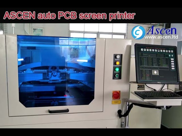
https://www.ascen.ltd/Products/Solder_paste_printer/513.html full auto PCB screen printer and SMT solder paste printing machine with Image and optical system,It is a very accurate fully automatic SMT stencil printer.automatic PCB screen printer main
https://www.ascen.ltd/Products/Solder_paste_printer/513.html full auto PCB screen printer and SMT solder paste printing machine with Image and optical system,It is a very accurate fully automatic SMT stencil printer.automatic PCB screen printer main
Career Center | Theni, Tamilnadu India | Engineering
NPI Engineer: • Playing a role as NPI leader of the Telecom, Aerospace & Server Products to introduce and run to qualify the engineering build from customer. • Conducting Weekly NPI meeting with the CFT team to review the progress of the NPI schedu
SMT Express, Issue No. 1 - from SMTnet.com Volume 1, Issue No. 1 Thursday, June 3, 1999 Tricks of the Trade Optimizing Time/Pressure Dispensing ofAdhesives by Chrys Shea Return to Previous Page Over the past
WINTECH SERVICE & MARKETING SDN BHD | https://www.wintech.my/product/solder-paste-printer-a9/
: SMT EQUIPMENT , SMT/AI EQUIPMENT , SOLDER PASTE PRINTER SOLDER PASTE PRINTER A9 SKU: A9 In Stock Model : A9 PCB Min Size : 50*50 mm PCB Max Size : 510*340 mm PCB Thickness
KingFei SMT Tech | https://www.smtspare-parts.com/quality-11936650-220v-50-60hz-solder-paste-inspection-table-top-3d-spi-7500-vision-ce
simulation function Powerful SPC function MARK deviation automatically corrected One-click back to the center of the screen Automatic Recognition Target This fully automatic 3D solder paste thickness tester can obtain 3D data of each point through the automatic XY stage moving/Z-axis image autofocus and laser scanning solder paste


