Industry Directory | Consultant / Service Provider
Specialists in high speed serial link architectures by providing innovative signal integrity & backplane solutions
Industry Directory | Manufacturer
SAFE-PCB Group is a global leading provider of time-critical and technologically complex PCBs, attractive for small and medium volume quick-turn orders. We provide 2-hour images for validation, same day production, and wide range.

MLT provides rigid and flexible circuit laser services including laser routing (excising), cavity skiving, coverlay/coverfilm routing, microvia drilling, ZIF Contours, Kapton window skives, depaneling, and marking. With 20 years experience, MLT has
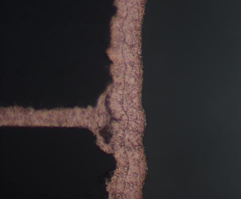
New Equipment | Test Equipment
Military-style laboratory services to validate bare boards for product assurance. Testing for delamination, voids, copper thickness, hole quality, proper stack-up, etc. Customer receives all cross-section pucks, boards and laboratory report with reco
Electronics Forum | Thu Aug 05 11:40:24 EDT 2004 | Dhanish
How do you perform stackup analysis for mechanical parts?I refer to some documents and it is very detail.
Electronics Forum | Wed Feb 26 21:44:52 EST 2003 | Paul Dansereau
I will be building a board, about 8 X 12 , .062" thick using a standard FR406 stackup. It has a variety of devices, including CCBGA , CBGA and PBGA's. Given the challenge of developing a reflow profile that will accomodate both ceramic and plastic BG
Industry News | 2017-08-06 19:39:48.0
The SMTA Capital Chapter is pleased to announce that Gerry Partida of Summit Interconnect, will present “Density, Advanced Materials and Cost Drivers Associated with Advanced Circuit Design, Fabrication and Assembly” at the upcoming Capital Expo and Tech Forum at Johns Hopkins University / Applied Physics Lab, Kossiakoff Center, on Thursday, August 24th.
Industry News | 2011-01-10 19:20:49.0
Plans are ramping up for IPC APEX EXPO™, April 10–14 in Las Vegas, aimed at meeting the needs of the engineers, PCB designers and manufacturing wizards who are tasked with bringing today’s consumer, industrial and high-reliability electronic products to life. With a focus on education, IPC will bring industry experts from around the world to lead 50 half-day professional development courses covering critical topics in design, PCB manufacturing, electronics assembly and test — supporting electronics manufacturers as they develop the next generation of electronics.
Technical Library | 2011-01-20 18:43:39.0
PCB stack-up is an important factor in determining the EMC performance of a product. A good stack-up can be very effective in reducing radiation from the loops on the PCB (differential-mode emission), as well as the cables attached to the board (common-mo
Technical Library | 2010-12-02 20:09:41.0
Planning the multilayer PCB stackup configuration is one of the most important aspects in achieving the best possible performance of a product. A correctly stacked PCB substrate ca effectively reduce electromagnetic emissions, crosstalk and also make the
Training Courses | | | PCB Design Courses
The PCB design courses teach students the process, techniques and tools needed to design layout of printed circuit boards.
Events Calendar | Wed Jul 26 00:00:00 EDT 2017 - Wed Jul 26 00:00:00 EDT 2017 | Chicago, Illinois USA
IPC Technical Education - Best Practices in Design
Events Calendar | Tue Jul 11 00:00:00 EDT 2023 - Tue Jul 11 00:00:00 EDT 2023 | Oshkosh, Wisconsin USA
Wisconsin Chapter In-Person Event: PCB Workshop and PCB Plant Tour
Manufacture and Characterization of a Novel Flip-Chip Package Z-interconnect Stack-up with RF Structures Manufacture and Characterization of a Novel Flip-Chip Package Z-interconnect Stack-up with RF Structures More and more chip packages need
Multilayer PCB Stackup Planning Multilayer PCB Stackup Planning Planning the multilayer PCB stackup configuration is one of the most important aspects in achieving the best possible performance of a product. A correctly stacked PCB substrate can
Whizz Systems | https://www.whizzsystems.com/custom-pcb-design/
. PCB Design Structure and Stackup 24 Layer PCB PCB size is 14.5×16 Inches and 110 mil thick Printed Circuit Board material is Isola 370 HR Layer stackup is 10 internal signal layers with mix dual and single strip line
| https://www.eptac.com/wp-content/uploads/eptac/datasheets/EPTAC_DataSheet_PCED.pdf
• Stackup Design with Fabrication Input • DFX, SI/PI and Layout Solvability • Constraints and Design Rules Checks (DRC) • Placement with Assembly/Manufacturing Considerations
.gif)


