New Equipment | Assembly Services
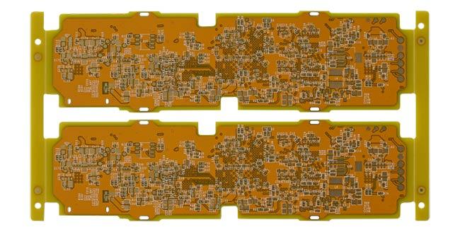
High Frequency PCB Material: SYTECH Layer Count: 4 layers PCB Thickness: 1.6mm Min. Trace / Space Outer: 0.1mm/0.1mm Min. Drilled Hole: 0.2mm Via Process: Tenting Vias Surface Finish: ENIG+OSP Product Features 1. DK needs to be tiny as well
New Equipment | Assembly Services
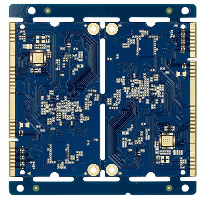
Thick-Copper PCB Material: Fr-4 Layer Count: 4 layers PCB Thickness: 1.4mm Min. Trace / Space Outer: 0.065mm Min. Drilled Hole: 0.2mm Via Process: Tenting Vias Surface Finish: ENIG Product Features Features: 1) Years of experience in half-
Electronics Forum | Fri Jun 09 17:34:08 EDT 2000 | Melanie Mulcahy
I need some information regarding the acceptability/unacceptability of using tented vias with LPI soldermask. Long story on all involved, but basically I have a board that I have had manufactured with no problems which has BGA/uBGA parts, tented via
Electronics Forum | Wed Jan 27 20:11:36 EST 2010 | plerma
What material is used to cap a via? Is it the > standard LPI Process/Material? we tent vias all the time, mostly to assist with assembly and the majority of the time outgassing is not a problem. What is the purpose in your case?
Industry News | 2019-11-05 22:07:01.0
Tenting a via refers to covering via with soldermask to enclose or skin over the opening. A via is a hole drilled into the PCB that allows multiple layers on the PCB to be connected to each other. A non tented via is just a via that is not covered with the soldermask layer. Leaving these vias exposed or covered has pros and cons depending on the your design and manufacturing requirements.
Industry News | 2018-10-18 10:40:04.0
Via Tent-Holes with Solder Mask
Technical Library | 2019-05-29 01:47:22.0
1.Vias near SMD pads: Solder can flow into the via after melted. As a result cold joint will appear in the end. Check the picture below. 2.Vias on SMD pads: Solder can flow into the via more easier after melted. Check the picture below. 3.Via opening without soldermask covered. When workers solder TH parts by hand, soldering iron can touch vias sometime, then tiny amounts molten solder will stay on vias. This can lead to electrical short easily. We recommend you make all vias tenting (covered by solder mask) if it is possible.
PCBNPI-Professional PCB Fab/PCB Assembly Service Provider From China
SMTnet Express, June 27, 2019, Subscribers: 32,092, Companies: 10,819, Users: 24,882 Advanced Cu Electroplating Process for Any Layer Via Fill Applications with Thin Surface Copper Credits: MacDermid Inc. Copper-filled micro-vias are a key


