New Equipment | Assembly Services
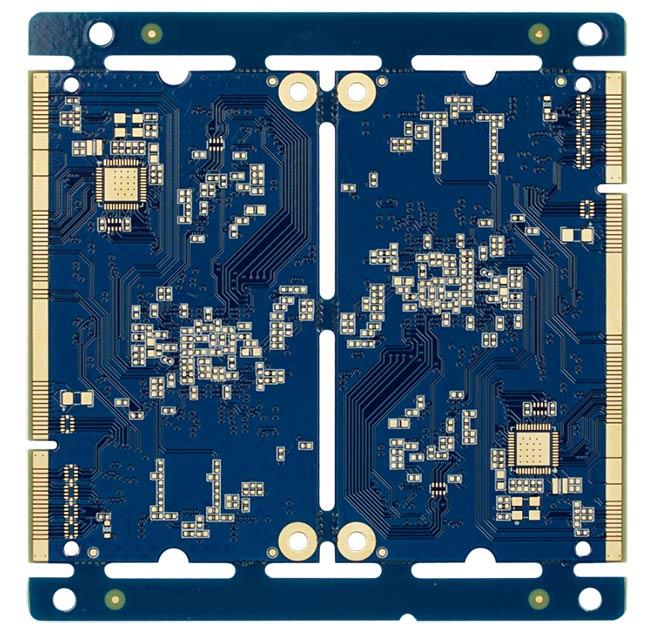
Thick-Copper PCB Material: Fr-4 Layer Count: 4 layers PCB Thickness: 1.4mm Min. Trace / Space Outer: 0.065mm Min. Drilled Hole: 0.2mm Via Process: Tenting Vias Surface Finish: ENIG Product Features Features: 1) Years of experience in half-
New Equipment | Assembly Services
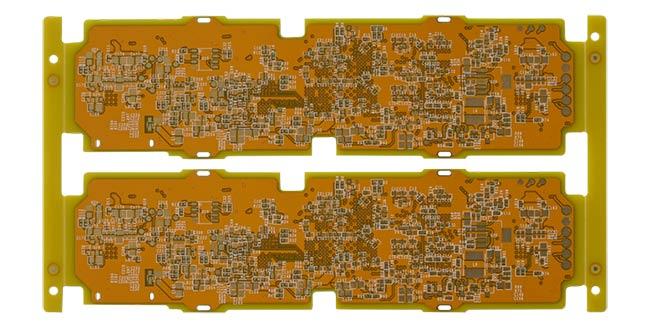
High Frequency PCB Material: SYTECH Layer Count: 4 layers PCB Thickness: 1.6mm Min. Trace / Space Outer: 0.1mm/0.1mm Min. Drilled Hole: 0.2mm Via Process: Tenting Vias Surface Finish: ENIG+OSP Product Features 1. DK needs to be tiny as well
Electronics Forum | Thu Jan 06 08:03:47 EST 2005 | davef
On solder in vias: It looks like the via are not solder masked well and pick-up solder either: * Solder coating ... OR * During leveling It's possible that the design specifies openings in the solder mask for these via. On solder in the unsupporte
Electronics Forum | Mon Jan 11 14:48:44 EST 2010 | davef
SR1000 is commonly used for tenting. Search the fine SMTnet Archives on : tenting Someone gave us this note. We have lost their name. It seems to be good advice. If Liquid Photo Image (LPI) solder mask is required, do not tent via holes. Tenting
Industry News | 2019-11-05 22:07:01.0
Tenting a via refers to covering via with soldermask to enclose or skin over the opening. A via is a hole drilled into the PCB that allows multiple layers on the PCB to be connected to each other. A non tented via is just a via that is not covered with the soldermask layer. Leaving these vias exposed or covered has pros and cons depending on the your design and manufacturing requirements.
Industry News | 2018-10-18 10:40:04.0
Via Tent-Holes with Solder Mask


