Industry Directory | Manufacturer
One-Stop Solution for PCB & Prototype Assembly Expanded PCB manufacturing capabilities to support advanced designs with demanding requirements including laser-drilled microvias, cavity boards, heavy copper up to 20 oz., via-in-pad
Industry Directory | Consultant / Service Provider / Manufacturer
Providing production and prototype, SEC offers advanced technologies like LED thermal management, heavy copper, PTFE for RFMW, open and internal cavities and blind and buried vias that are certified to a diverse set of industries.

New Equipment | Board Handling - Conveyors
Microcomputer control, stable and reliable. >LCD screen display, menu interface, the man-machine dialogue is convenient. >Many sound-light alarm function. >So can use standard feeder, strong commonality. >According to the thickness of the PCB so
_11.jpg)
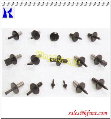
Smt I-pulse K01 nozzle used in pick and place machine Smt I-pulse K01 nozzle used in pick and place machine I-pulse series nozzles: 1.M1/M4 type:M001/M002/M003/M004/M005/M006/M012/M013/M017/M018/M019/M020/M021/M022/M031/M032/M033 2.M2 type:N001/N00
Electronics Forum | Sat Sep 14 01:34:19 EDT 2002 | Yngwie
I have the following questions on Via in Pad and want to understand each of them wrt : - complete Via in pad - partial encroachment - via partially in pad 1) What is the general feel for via in pad for upcoming designs? 2) What are the manufacturi
Electronics Forum | Wed Feb 27 19:55:13 EST 2002 | nifhail
Hi, I need help to understand further on the via in pad for 0402 requirement. If I were to do the DFM over the brd design which consist of 0402 with via on pad, what is the criteria that I should look for ? I learned that the via in pad does not wor

Used SMT Equipment | In-Circuit Testers
JDSU FST-2802-V6 Acterna Ethernet and Fibre Channel services module with FST2000 TestPad The FST2802 is a handheld Ethernet, Fibre Channel, and IP services test instrument designed to meet the needs of service providers for turning up and troub
Used SMT Equipment | In-Circuit Testers
JDSU FST-2802 Acterna Ethernet and Fibre Channel Services Module The FST-2802 is a handheld Ethernet, Fibre Channel, and IP services test instrument designed to meet the needs of service providers for turning up and troubleshooting these variou
Industry News | 2017-04-11 21:19:32.0
GPD Global offers versatile large format inline dispensing systems and stand-alone liquid dispense technologies for maximizing product yield. This is the largest standard PCB dispensing system platform in the industry.
Industry News | 2011-02-07 15:23:56.0
GPD Global will highlight its Positive Cavity Displacement (PCD) Dispensing at the upcoming SMTA Houston Expo & Tech Forum, scheduled to take place Thursday, March 3, 2011 at the Stafford Centre in Stafford, TX.
.jpg)
Parts & Supplies | SMT Equipment
Panasonic smt nozzles models: Panasonic MSR SMT NOZZLE Part Number Description 10468S0002 MSR - SMT NOZZLE - VVS (0.84 X 0.60) 10468S0003 - NZ. - VS (1.0 X 0.64) 10468S0004 -NZ. - S (1.6 X 1.06) 1046710134 -NZ. - M (1.60mm) 10467S0001 -NZ. - L
Parts & Supplies | SMT Equipment
Smt I-pulse nozzles used in pick and place machine I-pulse series nozzles: 1.M1/M4 type:M001/M002/M003/M004/M005/M006/M012/M013/M017/M018/M019/M020/M021/M022/M031/M032/M033 2.M2 type:N001/N002/N003/N004/N005/N006/N012/N013/N017/N018/N019/N020/N02
Technical Library | 2019-05-29 01:47:22.0
1.Vias near SMD pads: Solder can flow into the via after melted. As a result cold joint will appear in the end. Check the picture below. 2.Vias on SMD pads: Solder can flow into the via more easier after melted. Check the picture below. 3.Via opening without soldermask covered. When workers solder TH parts by hand, soldering iron can touch vias sometime, then tiny amounts molten solder will stay on vias. This can lead to electrical short easily. We recommend you make all vias tenting (covered by solder mask) if it is possible.
PCBNPI-Professional PCB Fab/PCB Assembly Service Provider From China
Technical Library | 2019-10-10 00:26:28.0
Voids are a plague to our electronics and must be eliminated! Over the last few years we have studied voiding in solder joints and published three technical papers on methods to "Fill the Void." This paper is part four of this series. The focus of this work is to mitigate voids for via in pad circuit board designs. Via holes in Quad Flat No-Lead (QFN) thermal pads create voiding issues. Gasses can come out of via holes and rise into the solder joint creating voids. Solder can also flow down into the via holes creating gaps in the solder joint. One method of preventing this is via plugging. Via holes can be plugged, capped, or left open. These via plugging options were compared and contrasted to each other with respect to voiding. Another method of minimizing voiding is through solder paste stencil design. Solder paste can be printed around the via holes with gas escape routes. This prevents gasses from via holes from being trapped in the solder joint. Several stencil designs were tested and voiding performance compared and contrasted. In many cases voiding will be reduced only if a combination of mitigation strategies are used. Recommendations for combinations of via hole plugging and stencil design are given. The aim of this paper is to help the reader to "Fill the Void."
To see more visit Pillarhouse here: https://www.pillarhouse.co.uk/products/selective-soldering-handload/pilot-handload Economical, compact, single point selective soldering system The all-new ultra-low-cost Pilot machine has been designed as an ent

The PCB Footprint Expert is a powerful CAD library development tool powered by our own proprietary CAD LEAP Technology (Libraries Enhanced with Automated Preferences). It is packed with very powerful advanced library management features that cuts foo
Training Courses | | | PCB Assembly Courses
The PCB assembly courses provide knowledge of different processes and equipment used in TH and SMT assembly of printed circuit boards.
Events Calendar | Mon Apr 23 00:00:00 EDT 2018 - Thu Apr 26 00:00:00 EDT 2018 | Shanghai, China
SMTA China East Conference 2018
Events Calendar | Thu Oct 03 00:00:00 EDT 2019 - Thu Oct 03 00:00:00 EDT 2019 | ,
IPC Tech Ed Webinar Series: Ball Grid Array (BGA) and Bottom Termination Component (BTC) Design and Assembly Challenges: Reflow Profiling to Achieve Low Defect Rates and Successful Assembly! – Part 2
Career Center | , | Engineering,Sales/Marketing,Technical Support
Applications Engineer with over 20 years of combined Manufacturing/Field Service/Applications Engineering experience in the SMT industry.
SMTnet Express, July 16, 2020, Subscribers: 28,512, Companies: 11,045, Users: 25,964 Via In Pad - Conductive Fill or Non-Conductive Fill? Credits: Advanced Circuits In the early 2000s the first fine-pitch ball grid array devices became popular
ASYMTEK Products | Nordson Electronics Solutions | https://www.nordson.com/en/divisions/march/products/plasma-treatment-systems/via-high-volume-series
. The VIA series plasma treatment systems utilize a patented plasma technology to produce superior uniformity at high throughputs. The VIA series for large-panel plasma processing is available in various chamber sizes, with choice of vertical or horizontal panel configurations
ORION Industries | http://orionindustries.com/pdfs/silpad400.pdf
. Special Thicknesses, Rolls and Sheets Sil-Pad 400 can be supplied on special order in a variety of thicknesses from .007 to .045 inches to fulfill special requirements of insulation path minimums or other spacing needs


