New Equipment | Design Services
The manufacturing factory at ACI includes a clean room, power electronics assembly and packaging laboratory. This specialized facility aids in the development of manufacturing and assembly technologies that can exploit the advantages of advanced mat
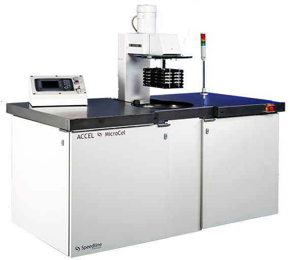
New Equipment | Cleaning Equipment
The first technology to use centrifugal energy to clean electronic circuit assemblies, precision parts, and semiconductor packages. The system offers unparalleled penetration, solubilization, and contaminant removal The MicroCel Centrifugal Cleanin
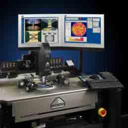
New Equipment | Test Equipment - Bond Testers
Fully integrated solution for automated wafer testing (up to 300 mm). The Condor Sigma W12 is specifically designed for precision shear testing and Cold Bump Pull (CBP) on wafer or at wafer level. The system has the largest X/Y and fastest stages av
All electronics plant including wafer fabrication, PCA and test
All electronics plant including wafer fabrication, PCA and test
Best-in-the-world measurements for 300mm wafers The Cascade Microtech S300 probe station sets the measurement standard for 300mm on-wafer test. Whether your application is device characterization and modeling, wafer-level reliability, design de-bug o
New Equipment | Test Equipment
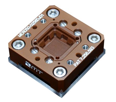
Multitest is able to offer you the contacting solution that best suits your application including: Kelvin test RF test tri-temp test MEMS test for testing: packages with pitches down to 0.25 mm packages on strips or
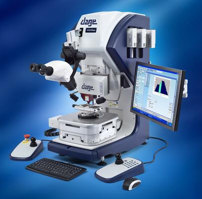
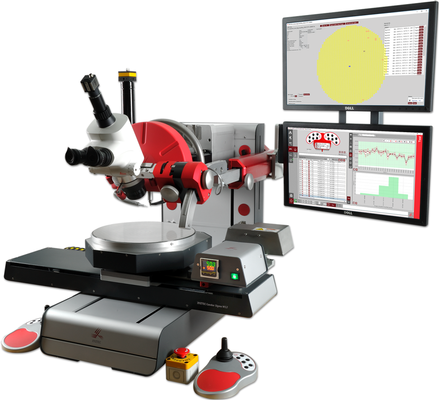
New Equipment | Test Equipment - Bond Testers
Nordson DAGE is the leading provider of award winning bond testing equipment. The second generation 4000Plus bondtester continues to be the most advanced bondtester on the market whilst the 4000 Optima is optimized for fast, accurate and reliable bon
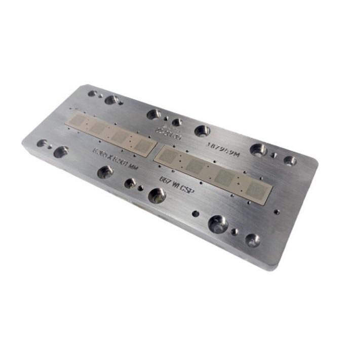
New Equipment | Board Handling - Pallets,Carriers,Fixtures
Benefits • Allows testing of RF devices at the wafer-level • Adaptable to wafer-level probing and singulated device testing for debug and characterization • Long life and extended maintenance intervals • Engineering analysis of WLCSP devices or K
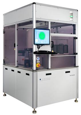
Highly Accurate Fully Automatic Wafer Inspection with Handling Unit For semiconductor assemblies, the requirement for a precise, thorough inspection for damage and defects during the production process is especially high. Wafers need non-destructive


