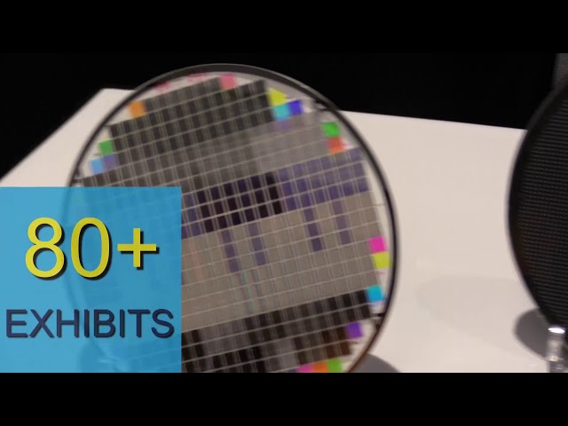
Why you should attend International Wafer-Level Packaging Conference, October 23 - 25, 2018 in San Jose, California, USA.

ACI Technologies Inc. (ACI) is a scientific research corporation dedicated to the advancement of electronics manufacturing processes and materials for The Department of Defense and industry. This video provides an overview of our commercial service
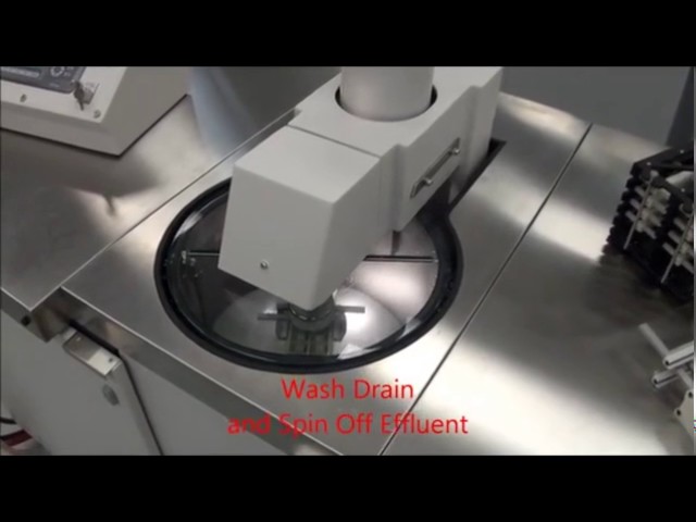
The first technology to use centrifugal energy to clean electronic circuit assemblies, precision parts, and semiconductor packages. The system offers unparalleled penetration, solubilization, and contaminant removal The MicroCel Centrifugal Cleanin
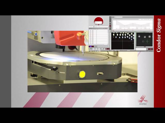
The Condor Sigma W12 is specifically designed for precision shear testing and Cold Bump Pull (CBP) on wafer or at wafer level. The system has the largest X/Y and fastest stages available in the industry, to reach all positions on the wafer with the t

This is the first in a series of 10-minute videos to introduce new users to the basics of machine vision technology. In this video, users will learn what machine vision is, how it is used in factory automation, and its four most common applications.
Covering the industrial chain of power semiconductor materials, chips, modules, equipment and other industries, dozens of enterprises from home and abroad participated in the exhibition. This series of products can control the welding cavity rate of
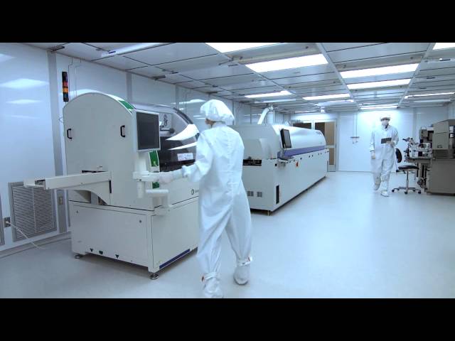
The Microelectronics Lab was established to meet the rising need for advanced systems development and packaging to address the emerging challenges and issues facing today’s electronics assemblies. Advanced design and modeling software enables STI to
| 1 |

.gif)


