New Equipment | Fabrication Services
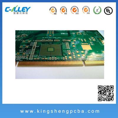
Our Service PCB Assembly and PCB&PCBA design are our main business.We are able to undertake a high quality Printed Circuit Board Assembly on competitive prices and flexible conditions.We are a complete “One- Stop” resource for printed circuit board
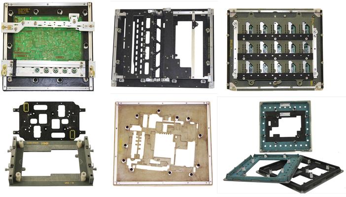
New Equipment | Board Handling - Pallets,Carriers,Fixtures
Our Wave Solder Fixtures increase productivity and eliminate defects in your pcb assembly process. This type of fixture supports the pcb on all four sides eliminating warpage that can cause solder skips and bridges or pcb flooding. They also elim
Electronics Forum | Wed Jul 02 03:24:35 EDT 2003 | ramanandkini
did you check with lackwere peters? My frined told me that they have some coatings for this application.
Electronics Forum | Wed Jul 02 19:20:43 EDT 2003 | teamcanada
Have you looked into Kapton tape as a protectant?
Industry News | 2013-10-28 16:31:54.0
IPC Conference on Solder and Reliability: Materials, Processes and Tests, November 13–14 in Costa Mesa, Calif.
Industry News | 2013-02-20 18:54:10.0
IPC — Association Connecting Electronics Industries® presented Committee Leadership, Distinguished Committee Service and Special Recognition Awards at IPC APEX EXPO® at the San Diego Convention Center.
Technical Library | 2020-08-27 01:22:45.0
Initially adopted internal specifications for acceptance of printed circuit boards (PCBs) used for wire bonding was that there were no nodules or scratches allowed on the wirebond pads when inspected under 20X magnification. The nodules and scratches were not defined by measurable dimensions and were considered to be unacceptable if there was any sign of a visual blemish on wire-bondable features. Analysis of the yield at a PCB manufacturer monitored monthly for over two years indicated that the target yield could not be achieved, and the main reasons for yield loss were due to nodules and scratches on the wirebonding pads. The PCB manufacturer attempted to eliminate nodules and scratches. First, a light-scrubbing step was added after electroless copper plating to remove any co-deposited fine particles that acted as a seed for nodules at the time of copper plating. Then, the electrolytic copper plating tank was emptied, fully cleaned, and filtered to eliminate the possibility of co-deposited particles in the electroplating process. Both actions greatly reduced the density of the nodules but did not fully eliminate them. Even though there was only one nodule on any wire-bonding pad, the board was still considered a reject. To reduce scratches on wirebonding pads, the PCB manufacturer utilized foam trays after routing the boards so that they did not make direct contact with other boards. This action significantly reduced the scratches on wire-bonding pads, even though some isolated scratches still appeared from time to time, which caused the boards to be rejected. Even with these significant improvements, the target yield remained unachievable. Another approach was then taken to consider if wire bonding could be successfully performed over nodules and scratches and if there was a dimensional threshold where wire bonding could be successful. A gold ball bonding process called either stand-off-stitch bonding (SSB) or ball-stitch-on-ball bonding (BSOB) was used to determine the effects of nodules and scratches on wire bonds. The dimension of nodules, including height, and the size of scratches, including width, were measured before wire bonding. Wire bonding was then performed directly on various sizes of nodules and scratches on the bonding pad, and the evaluation of wire bonds was conducted using wire pull tests before and after reliability testing. Based on the results of the wire-bonding evaluation, the internal specification for nodules and scratches for wirebondable PCBs was modified to allow nodules and scratches with a certain height and a width limitation compared to initially adopted internal specifications of no nodules and no scratches. Such an approach resulted in improved yield at the PCB manufacturer.
ASYMTEK Products | Nordson Electronics Solutions | https://www.nordson.com/en/divisions/dage/test-types/first-bond-ball-pull-stud-bump-pull?con=t&page=2
. First bond ball pull testing is predominantly used as an alternative to ball shear testing to verify copper wire ball bonds which is increasingly being as an alternative to gold for semiconductor interconnects
Baja Bid | https://bajabid.com/online-smt-auction-featuring-sypris-electronics/
; Ling Electronics A540 Shaker; Royce Model 550 Gold Bond Test Instrument; MACHINE SHOP EQUIPMENT including Bridgeport Mills; Cincinnati Horizontal Milling Machine

.gif)
