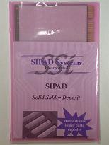
SIPAD Solid Solder Deposit (ssd) is a Siemens patented process that pre loads the pc board surface mount pads with solder in a solid form. Boards are printed, reflowed without components producing a predictable repeatable meniscus. SIPAD boards a
New Equipment | Assembly Services
China Double Sided Circuit Boards Fabricaiton and Assembly PCBA Turnkey Manufacturer 2 Layers circuit boards PCB FR4 1.6mm PCB fabrication and assembly 1oz PCB copper thickness Shenzhen PCB and PCBA manufacturer China turnkey contract electroni

SIPAD Systems Incorporated (SSi) is the Exclusive Supplier of SIPAD solid solder deposit in North America and the only SIPAD Solid Solder Deposit (SSD) coating service bureau in the world. SIPAD Systems Inc. supplies SIPAD solid solder coating servi
Industry News | 2019-11-05 22:08:21.0
Via in pad is the design practice of placing a via in the copper landing pad of a component. Compared to standard PCB via routing, via in pad allows a design to use smaller component pitch sizes and further reduce the PCBs overall size. With component manufactures pushing smaller parts every year and the demand from consumers for smaller devices, the usage of via in pad practices by hardware engineers have become more commonplace. In this article, we will discuss the differences between via in pad and traditional vias, when should you use via in pad, and how to design for it.
Industry News | 2018-10-18 10:40:04.0
Via Tent-Holes with Solder Mask
Electronics Forum | Wed Feb 16 09:33:09 EST 2000 | Kurt Waskow
Interested in information regarding PCB soldermask tenting over vias within a BGA layout. Is this a common practice to reduce the occurrence of shorts, are there any reliability concerns? Thanks!
Electronics Forum | Wed Feb 16 09:33:09 EST 2000 | Kurt Waskow
Interested in information regarding PCB soldermask tenting over vias within a BGA layout. Is this a common practice to reduce the occurrence of shorts, are there any reliability concerns? Thanks!
Electronics Forum | Mon Feb 21 08:33:53 EST 2000 | Tony Di Mauro
Kurt, When I was working in a captive manufacturing house we had been to migrate toward tenting all vias under the BGA to eliminate not only shorts but insufficient (Starved) joints. Tony
Electronics Forum | Mon Feb 21 08:33:53 EST 2000 | Tony Di Mauro
Kurt, When I was working in a captive manufacturing house we had been to migrate toward tenting all vias under the BGA to eliminate not only shorts but insufficient (Starved) joints. Tony
Electronics Forum | Fri Oct 15 10:35:44 EDT 2004 | russ
sounds like you have a very thin layer of mask on some pads to me. Russ


