Technical Library | 2013-01-18 02:42:14.0
ENIG (Electroless Nickel/Immersion Gold) is to deposit nickel gold plating which has good solderability, wear resistance , leveling appearance and small electric resistance. It included 4 steps that are pretreatment, immersion nickel, immersion gold and Post treatment...

PCB Prototype - 2 Layer, Hard Gold Plating 30u", Controlled Deep Cut/Milling And Special CNC - 2 layer, hard gold plating 30u", controlled deep cut/milling and special CNC. - Red solder mask.
Career Center | Dana Point, California USA | Sales/Marketing
We are currently seeking sales reps nationwide for this rapidly growing supplier of printed circuit boards (since 1986)with facilities in southern CA and eight PCB facilities in China and Taiwan, all ISO 9002 certified and UL94V-0 approved, some are
Industry Directory | Manufacturer
PCB Repairs of all kinds including-Solder on Tab (Solder Removal, Gold Plating), PTH & Delam repairs, etc.
Technical Library | 2014-08-07 15:13:44.0
Gold embrittlement in SnPb solder is a well-known failure mechanism in electronic assembly. To avoid this issue, prior studies have indicated a maximum gold content of three weight percent. This study attempts to provide similar guidance for Pb-free (SAC305) solder. Standard surface mount devices were assembled with SnPb and SAC305 solder onto printed boards with various thicknesses of gold plating. The gold plating included electroless nickel immersion gold (ENIG) and electrolytic gold of 15, 25, 35, and 50 microinches over nickel. These gold thicknesses resulted in weight percentages between 0.4 to 7.0 weight percent.
Industry Directory | Manufacturer
2Layers - 18Layers ;HASL, OSP, Gold plating, immersion Gold/Silver/Tin, removable mask, gold-finger, carbon ink;Conact Person:Rene E-mail:rene@speedingcircuit.com Website:www.speedingcircuit.com
New Equipment | Fabrication Services
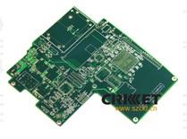
Base Material: FR4 Layer count: 4 layer Board thickness: 1.6mm Copper Thickness:1 oz Surface finish: nickel gold plating Soldermask Colors: Green Size:159.25*182/1up
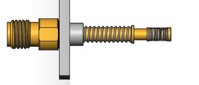
Mechanical data Working stroke: 4,3 mm (.169) Maximum stroke: 6,35 mm (.250) Spring force at work. stroke: 0,8 N (2.9oz) Materials Plunger: Steel or BeCu, gold-plated Barrel: Bronze, gold-plated Spring: Steel, gold-plated Receptacle: Nickel-silver,
Industry News | 2016-06-10 09:45:09.0
Cranston RI - Technic is pleased to announce the installation of the TechniPad Electroless Palladium process AT7015 at Gold Plating Services (GPS) in Santa Clara CA. GPS is a contract plating service specializing in precious metal plating for the printed circuit board industry.
Technical Library | 1999-05-07 11:28:39.0
There are many things that can go wrong when soldering to gold plate over nickel surfaces. First of all, we know that gold and solder are not good friends, as any time solder comes into contact with gold, something seems to go wrong. Either the solder bonds to the gold and eventually pulls off as the tin and gold cross-migrate, leaving voids; or the solder completely removes the gold and is expected to bond to the metal which was under the gold.


