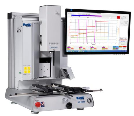
New Equipment | Rework & Repair Equipment
Patented Inductive-Convection Heating Technology Provides Ultimate Thermal Performance Conventional resistance coil heating technology has been successfully used in convective rework stations for decades to install and remove a variety of BGA, QFN,
Technical Library | 2023-07-25 16:25:56.0
This paper address two significant applications of stencils in advance packaging field: 1. Ultra-Thin stencils for miniature component (0201m) assembly; 2. Deep Cavity stencils for embedded (open cavity) packaging. As the world of electronics continues to evolve with focus on smaller, lighter, faster, and feature-enhanced high- performing electronic products, so are the requirement for complex stencils to assemble such components. These stencil thicknesses start from less than 25um with apertures as small as 60um (or less). Step stencils are used when varying stencil thicknesses are required to print into cavities or on elevated surfaces or to provide relief for certain features on a board. In the early days of SMT assembly, step stencils were used to reduce the stencil thickness for 25 mil pitch leaded device apertures. Thick metal stencils that have both relief-etch pockets and reservoir step pockets are very useful for paste reservoir printing. Electroform Step-Up Stencils for ceramic BGA's and RF Shields are a good solution to achieve additional solder paste height on the pads of these components as well as providing exceptional paste transfer for smaller components like uBGAs and 0201s. As the components are getting smaller, for example 0201m, or as the available real estate for component placement on a board is getting smaller – finer is the aperture size and the pitch on the stencils. Aggressive distances from step wall to aperture are also required. Ultra-thin stencils with thicknesses in the order of 15um-40um with steps of 15um are used to obtain desired print volumes. Stencils with thickness to this order can be potential tools even to print for RDLs in the package.
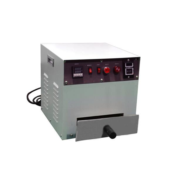
1, All the main parts of the equipment are imported parts, long service life. 2, using the upper and lower two temperature control area, using PID automatic fuzzy temperature control system, high precision temperature control, high stability, tempera
Technical Library | 2020-10-14 14:33:36.0
Epoxy based adhesives are prevalent interface materials for all levels of electronic packaging. One reason for their widespread success is their ability to accept fillers. Fillers allow the adhesive formulator to tailor the electrical and thermal properties of a given epoxy. Silver flake allow the adhesive to be both electrically conductive and thermally conductive. For potting applications, heat sinking, and general encapsulation where high electrical isolation is required, aluminum oxide has been the filler of choice. Today, advanced Boron Nitride filled epoxies challenge alternative thermal interface materials like silicones, greases, tapes, or pads. The paper discusses key attributes for designing and formulating advanced thermally conductive epoxies. Comparisons to other common fillers used in packaging are made. The filler size, shape and distribution, as well as concentration in the resin, will determine the adhesive viscosity and rheology. Correlation's between Thermal Resistance calculations and adhesive viscosity are made. Examples are shown that determination of thermal conductivity values in "bulk" form, do not translate into actual package thermal resistance. Four commercially available thermally conductive adhesives were obtained for the study. Adhesives were screened by shear strength measurements, Thermal Cycling ( -55 °C to 125 °C ) Resistance, and damp heat ( 85 °C / 85 %RH ) resistance. The results indicate that low modulus Boron Nitride filled epoxies are superior in formulation and design. Careful selection of stress relief agents, filler morphology, and concentration levels are critical choices the skilled formulator must make. The advantages and limitations of each are discussed and demonstrated.
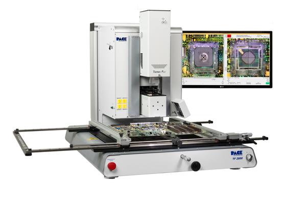
New Equipment | Rework & Repair Equipment
Patented Inductive-Convection Heating Technology Provides Ultimate Thermal Performance Conventional resistance coil heating technology has been successfully used in convective rework stations for decades to install and remove a variety of BGA, QFN,
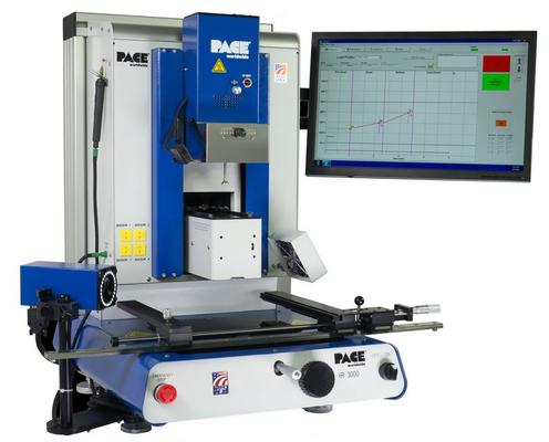
New Equipment | Rework & Repair Equipment
Production BGA Installation & Rework WITHOUT the Expensive Nozzles! The IR 3000 is the most advanced BGA rework system available on the market today. It can easily install and remove BGA, QFN, µBGA/CSP, Flip Chip and other SMD's. Featuring a 500W in
Technical Library | 2009-11-05 11:17:32.0
Head-in-pillow (HiP), also known as ball-and-socket, is a solder joint defect where the solder paste deposit wets the pad, but does not fully wet the ball. This results in a solder joint with enough of a connection to have electrical integrity, but lacking sufficient mechanical strength. Due to the lack of solder joint strength, these components may fail with very little mechanical or thermal stress. This potentially costly defect is not usually detected in functional testing, and only shows up as a failure in the field after the assembly has been exposed to some physical or thermal stress.
Training Courses | | | IPC-7711/7721 Specialist (CIS)
The Certified IPC-7711/7721 Specialist (CIS) training focuses on rework of electronic assemblies and repair and modification of printed boards and electronic assemblies.
Industry News | 2019-11-05 22:08:21.0
Via in pad is the design practice of placing a via in the copper landing pad of a component. Compared to standard PCB via routing, via in pad allows a design to use smaller component pitch sizes and further reduce the PCBs overall size. With component manufactures pushing smaller parts every year and the demand from consumers for smaller devices, the usage of via in pad practices by hardware engineers have become more commonplace. In this article, we will discuss the differences between via in pad and traditional vias, when should you use via in pad, and how to design for it.
Industry Directory | Consultant / Service Provider
CAD Design Software products run in the AutoCAD environment.


