Technical Library | 2020-09-02 22:14:36.0
The demand for miniaturization and higher density electronic products has continued steadily for years, and this trend is expected to continue, according to various semiconductor technology and applications roadmaps. The printed circuit board (PCB) must support this trend as the central interconnection of the system. There are several options for fine line circuitry. A typical fine line circuit PCB product using copper foil technology, such as the modified semi-additive process (mSAP), uses a thin base copper layer made by pre-etching. The ultrathin copper foil process (SAP with ultrathin copper foil) is facing a technology limit for the miniaturization due to copper roughness and thickness control. The SAP process using sputtered copper is a solution, but the sputtering process is expensive and has issues with via plating. SAP using electroless copper deposition is another solution, but the process involved is challenged to achieve adequate adhesion and insulation between fine-pitch circuitries. A novel catalyst system--liquid metal ink (LMI)--has been developed that avoids these concerns and promotes a very controlled copper thickness over the substrate, targeting next generation high density interconnect (HDI) to wafer-level packaging substrates and enabling 5-micron level feature sizes. This novel catalyst has a unique feature, high density, and atomic-level deposition. Whereas conventional tin-palladium catalyst systems provide sporadic coverage over the substrate surface, the deposited catalyst covers the entire substrate surface. As a result, the catalyst enables improved uniformity of the copper deposition starting from the initial stage while providing higher adhesion and higher insulation resistance compared to the traditional catalysts used in SAP processes. This article discusses this new catalyst process, which both proposes a typical SAP process using the new catalyst and demonstrates the reliability improvements through a comparison between a new SAP PCB process and a conventional SAP PCB process.

Great Lakes Engineering boasts over 20 years in chemical etching technology. In essence, this is the process of printing (photo-plotting) a pattern on a metal foil and immersing it in a precise combination of chemistry in order to eat through (etch t
Technical Library | 2010-07-08 19:49:59.0
Aging characteristics of new lead free solder alloys are in question by many experts because of higher amount of tin’s effect on the diffusion of other metals, primarily copper, to create undesirable boundary intermetallics over long periods of time and even moderately elevated temperatures. A primary layer of intermetallics, Cu6Sn5 forms as the liquid solder makes contact with the solid copper substrate. This reaction however ceases as the solder temperature falls below that of liquidus. A secondary intermetallic Cu3Sn1, an undesirable weak and brittle layer, is thought to form over time and may be accelerated by even mildly elevated temperatures in electronic modules such as laptops under power. This project was designed to quantify the growth rate of Cu3Sn1 over an extended period of time in a thermal environment similar to a laptop in the power on mode.
Industry News | 2016-05-21 08:04:11.0
Oak-Mitsui are proud to announce an expanded strategic partnership adding Oak Mitsui’s proprietary ABC (aluminum bonded copper) to Insulectro’s premier product portfolio including CAC (copper aluminum copper). By leveraging their bicoastal manufacturing locations, ABC will continue to manufacture its bonded product in Hoosick Falls, NY and Insulectro will continue to manufacture CAC at its facility in Lake Forest, CA. The complete line of Oak-Mitsui copper foils, on CAC and ABC, will be available in Insulectro’s inventory by June 17, 2016.
Technical Library | 2016-07-07 15:37:18.0
How susceptible are the metals used in modern electronics manufacturing to corrosion by common beverages? This is a question of interest, especially to manufacturers, retailers and to a certain extent end customers. In this study the dissolution of aluminum, copper, gold, iron, lead, nickel, SAC305 solder, silver, tin and zinc was examined. Individual foils of these materials were fully immersed in one of sixteen chosen beverages and heated for 3 days at 40°C. The resulting solutions were analyzed using ICP-OES. The data were examined in light of the known pH, conductivity and ionic contents of the beverages, determined in previous work. Conclusions about the relative susceptibility to corrosion of the various metals and the corrosive power of the different beverages are made.
Technical Library | 2020-01-09 00:00:30.0
PCBs have a wide range of applications in electronics where they are used for electric signal transfer. For a multilayer build-up, thin copper foils are alternated with epoxy-based prepregs and laminated to each other. Adhesion between copper and epoxy composites is achieved by technologies based on mechanical interlocking or chemical bonding, however for future development, the understanding of failure mechanisms between these materials is of high importance. In literature, various interfacial failures are reported which lead to adhesion loss between copper and epoxy resins. This review aims to give an overview on common coupling technologies and possible failure mechanisms. The information reviewed can in turn lead to the development of new strategies, enhancing the adhesion strength of copper/epoxy joints and, therefore, establishing a basis for future PCB manufacturing.
Pyralux® LF Copper-clad Laminate DuPont™ Pyralux® LF has been an industry standard in high reliability applications in the avionics industry for over 30 years and has a proven record of consistency and dependability and is ideal for aerospace and m
Technical Library | 2021-11-03 16:49:59.0
Ultrathin bare die chips were soldered using a novel soldering technology. Using homogeneous flash light generated by high-power xenon flash lamp the dummy components and the bare die NFC chips were successfully soldered to copper tracks on polyimide (PI) and polyethylene terephthalate (PET) flex foils by using industry standard Sn-Ag-Cu lead free alloys. Due to the selectivity of light absorption, a limited temperature increase was observed in the PET substrates while the chip and copper tracks were rapidly heated to a temperatures above the solder melting temperature. This allowed to successfully soldered components onto the delicate polyethylene foil substrates using lead-free alloys with liquidus temperatures above 200 °C. It was shown that by preheating components above the decomposition temperature of solder paste flux with a set of short low intensity pulses the processing window could be significantly extended compared to the process with direct illumination of chips with high intensity flash pulse. Furthermore, it was demonstrated that with localized tuning of pulse intensity components having different heat capacity could be simultaneously soldered using a single flash pulse.
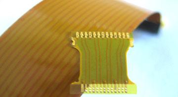
Technical Library | 2012-12-26 20:18:50.0
①Single side The basic flexible printed circuit board is used of substrate of single side pcb materials and coated coverlay after finishing printed. ②Double sided That is made of substrates of double sided printed circuit board with double surface coated coverlays after finishing printed. ③Single copper foil with double coverlays Single copper foil coated different coverlays with double surface after finishing printed. ④Air gap Laminating two single printed circuit board together with no glue and bare design to meet high flexibility requirements. ⑤Multilayer That is designed for three and above circuit layers by laminating single side printed circuit board or double sided printed circuit board. ⑥COF IC chips and electronic components are installed on the flexible circuit board directly. ⑦Rigid-Flexible PCB Combined to rigid PCB with supporting and flexible PCB with high flexibility.
.jpg)
Layer Count: 8L Board Thickness: 1.0mm Panel Dimension:190*86mm/2up Material: S1141 Copper on board surface: 35μm Min Hole Diameter: 0.1mm Min line Width/Space: 8/8mil Surface Finish: ENIG+Selective OSP in BGA area This quick turn PCB is manufacture

.gif)


