Technical Library | 2023-06-02 14:13:02.0
This work examines the use of dual-material fused filament fabrication for 3D printing electronic componentsand circuits with conductive thermoplastic filaments. The resistivity of traces printed fromconductive thermoplastic filaments made with carbon-black, graphene, and copper as conductive fillerswas found to be 12, 0.78, and 0.014 ohm cm, respectively, enabling the creation of resistors with valuesspanning 3 orders of magnitude. The carbon black and graphene filaments were brittle and fracturedeasily, but the copper-based filament could be bent at least 500 times with little change in its resistance.Impedance measurements made on the thermoplastic filaments demonstrate that the copper-based filamenthad an impedance similar to a copper PCB trace at frequencies greater than 1 MHz. Dual material3D printing was used to fabricate a variety of inductors and capacitors with properties that could bepredictably tuned by modifying either the geometry of the components, or the materials used to fabricatethe components. These resistors, capacitors, and inductors were combined to create a fully 3Dprinted high-pass filter with properties comparable to its conventional counterparts. The relatively lowimpedance of the copper-based filament enabled its use for 3D printing of a receiver coil for wirelesspower transfer. We also demonstrate the ability to embed and connect surface mounted components in3D printed objects with a low-cost ($1000 in parts), open source dual-material 3D printer. This work thusdemonstrates the potential for FFF 3D printing to create complex, three-dimensional circuits composedof either embedded or fully-printed electronic components.

Technical Library | 2019-02-13 13:45:11.0
Development of information and telecommunications network is outstanding in recent years, and it is required for the related equipment such as communication base stations, servers and routers, to process huge amount of data in no time. As an electrical signal becomes faster and faster, how to prevent signal delay by transmission loss is a big issue for Printed Circuit Boards (PCB) loaded on such equipments. There are two main factors as the cause of transmission loss; dielectric loss and conductor loss. To decrease the dielectric loss, materials having low dielectric constant and low loss tangent have been developed. On the other hand, reducing the surface roughness of the copper foil itself to be used or minimizing the surface roughness by modifying surface treatment process of the conductor patterns before lamination is considered to be effective in order to decrease the conductor loss. However, there is a possibility that reduction in the surface roughness of the conductor patterns will lead to the decrease in adhesion of conductor patterns to dielectric resin and result in the deterioration of reliability of PCB itself. In this paper, we will show the evaluation results of adhesion performance and electrical properties using certain type of dielectric material for high frequency PCB, several types of copper foil and several surface treatment processes of the conductor patterns. Moreover, we will indicate a technique from the aspect of surface treatment process in order to ensure reliability and, at the same time, to prevent signal delay at the signal frequency over 20 GHz.
Thermally Managed � Heat Dissipating PCB�s (Printed Circuit Boards) By STABLCOR Corporation STABLCOR TM Printed Circuit Board Material Product Information STABLCOR Corporation has developed a new printed circuit board technology that has the followin
New Equipment | Assembly Services
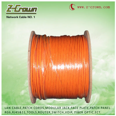
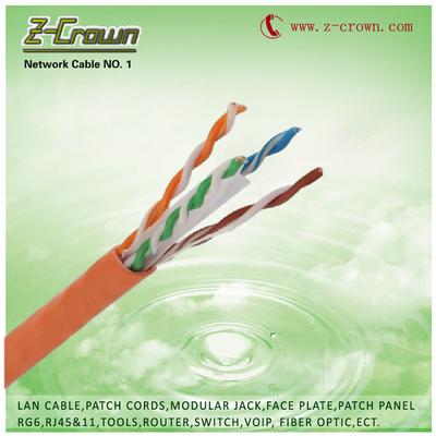
Factory supply cable utp cat5e and cat6 lan cable 305m (Rhonda(at)z-crown.com cable utp cat5e: 1.Conductor:24AWG,bare copper 0.51 +/-0.01 mm, 2.Insulation: High density polyethylene, minimum thickness of 0.19 mm 3.Conductor diameter 0.92 +/- 0
New Equipment | Assembly Services
Factory supply cable utp cat5e and cat6 lan cable 305m (Rhonda(at)z-crown.com cable utp cat5e: 1.Conductor:24AWG,bare copper 0.51 +/-0.01 mm, 2.Insulation: High density polyethylene, minimum thickness of 0.19 mm 3.Conductor diameter 0.92 +/- 0

Bob Willis videos show you How to Do It each month. This month we talk about adhesion testing like copper foil, plated copper on PCBs or conformal coating adhesion to board assemblies. Adhesion testing can be used for many different materials and in
Technical Library | 2019-06-20 00:09:49.0
It is well known that during service the layer of Cu6Sn5 intermetallic at the interface between the solder and a Cu substrate grows but the usual concern has been that if this layer gets too thick it will be the brittleness of this intermetallic that will compromise the reliability of the joint, particularly in impact loading. There is another level of concern when the Cu-rich Cu3Sn phase starts to develop at the Cu6Sn5/Cu interface and an imbalance in the diffusion of atomic species, Sn and Cu, across that interface results in the formation at the Cu3Sn/Cu interface of Kirkendall voids, which can also compromise reliability in impact loading. However, when, as is the case in some microelectronics, the copper substrate is thin in relation to the volume of solder in the joint an overriding concern is that all of the Cu will be consumed by reaction with Sn to form these intermetallics.This paper reports an investigation into the kinetics of the growth of the interfacial intermetallic, and the consequent reduction in the thickness of the Cu substrate in solder joints made with three alloys, Sn-3.0Ag-0.5Cu, Sn-0.7Cu-0.05Ni and Sn-1.5Bi-0.7Cu-0.05Ni.

Tachyon-100G laminate materials are designed for very high-speed digital applications up to and beyond speeds of 100 Gb/s. Tachyon 100-G materials exhibit exceptional electrical properties that are very stable over a broad frequency and temperature
Industry News | 2011-01-18 13:46:21.0
Time and again, a major challenge lies in attaching integrated circuits (ICs) to highly integrated circuit board substrates in a space-saving manner. Würth Elektronik took this challenge on and found an ideal solution with the ESC (encapsulated solder connection) process. The chips are soldered and at the same time glued 'face-down" in their exact position.


