◆ Contact Me SALES MANAGER : YUKI EMAIL: SALES15@AMIKON.CN SKYPE/ WHATSAPP: 86 17359287459 ◆ About Amikon Limited Amikon Limited has a large selection of industrial electronic components including new and discontinued. These range from thi
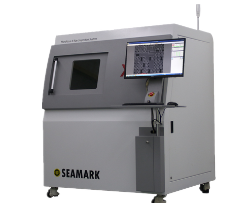
Product Application: X-Ray inspection is a method of non-destructive testing where many types of manufactured components can be examined to verify the internal structure via the penetration power from X-Ray. Seamark Zhuomao X-6600 X-ray inspection
Industry News | 2018-10-18 10:40:04.0
Via Tent-Holes with Solder Mask
New Equipment | Assembly Services
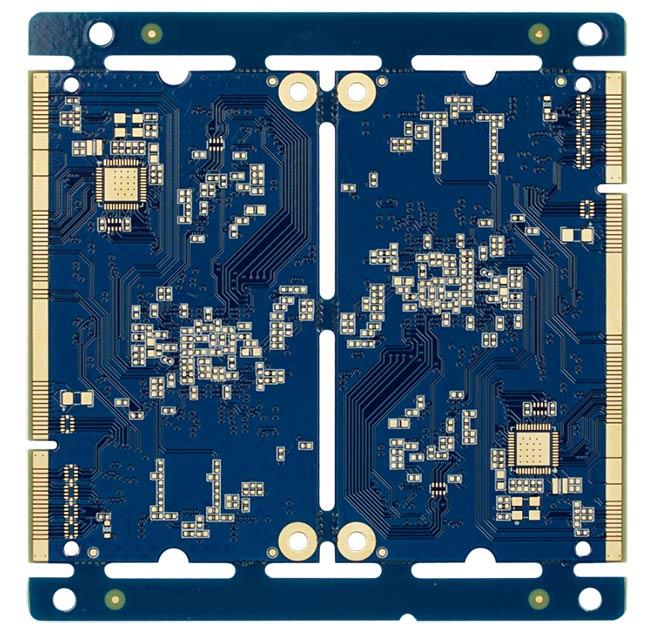
Thick-Copper PCB Material: Fr-4 Layer Count: 4 layers PCB Thickness: 1.4mm Min. Trace / Space Outer: 0.065mm Min. Drilled Hole: 0.2mm Via Process: Tenting Vias Surface Finish: ENIG Product Features Features: 1) Years of experience in half-
New Equipment | Assembly Services
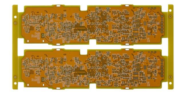
High Frequency PCB Material: SYTECH Layer Count: 4 layers PCB Thickness: 1.6mm Min. Trace / Space Outer: 0.1mm/0.1mm Min. Drilled Hole: 0.2mm Via Process: Tenting Vias Surface Finish: ENIG+OSP Product Features 1. DK needs to be tiny as well
Technical Library | 2019-05-29 01:47:22.0
1.Vias near SMD pads: Solder can flow into the via after melted. As a result cold joint will appear in the end. Check the picture below. 2.Vias on SMD pads: Solder can flow into the via more easier after melted. Check the picture below. 3.Via opening without soldermask covered. When workers solder TH parts by hand, soldering iron can touch vias sometime, then tiny amounts molten solder will stay on vias. This can lead to electrical short easily. We recommend you make all vias tenting (covered by solder mask) if it is possible.
PCBNPI-Professional PCB Fab/PCB Assembly Service Provider From China
Industry News | 2018-10-18 08:29:16.0
How to Prevent Short Circuits to Ground in QFN Components?
Parts & Supplies | Circuit Board Assembly Products
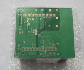
1). 100mm x 98mm/1up, FR-4, 2). 1mm +/-0.1mm,6 Layers 3). 1oz copper finished 3). Green solder mask/white legend 4). Min. hole 0.15mm, 4/4 mil track/gap 5). Blind via layer 1-2, via-in-pad. 6). Immersion gold surface finish
Technical Library | 2020-07-15 18:49:03.0
Via Filling • Through Hole Vias - IPC-4761 – Plugging – Filling – Filled & Capped • MicroviaFilling and Stacked Vias
Industry News | 2019-11-05 22:08:21.0
Via in pad is the design practice of placing a via in the copper landing pad of a component. Compared to standard PCB via routing, via in pad allows a design to use smaller component pitch sizes and further reduce the PCBs overall size. With component manufactures pushing smaller parts every year and the demand from consumers for smaller devices, the usage of via in pad practices by hardware engineers have become more commonplace. In this article, we will discuss the differences between via in pad and traditional vias, when should you use via in pad, and how to design for it.


