Technical Library | 2020-08-27 01:22:45.0
Initially adopted internal specifications for acceptance of printed circuit boards (PCBs) used for wire bonding was that there were no nodules or scratches allowed on the wirebond pads when inspected under 20X magnification. The nodules and scratches were not defined by measurable dimensions and were considered to be unacceptable if there was any sign of a visual blemish on wire-bondable features. Analysis of the yield at a PCB manufacturer monitored monthly for over two years indicated that the target yield could not be achieved, and the main reasons for yield loss were due to nodules and scratches on the wirebonding pads. The PCB manufacturer attempted to eliminate nodules and scratches. First, a light-scrubbing step was added after electroless copper plating to remove any co-deposited fine particles that acted as a seed for nodules at the time of copper plating. Then, the electrolytic copper plating tank was emptied, fully cleaned, and filtered to eliminate the possibility of co-deposited particles in the electroplating process. Both actions greatly reduced the density of the nodules but did not fully eliminate them. Even though there was only one nodule on any wire-bonding pad, the board was still considered a reject. To reduce scratches on wirebonding pads, the PCB manufacturer utilized foam trays after routing the boards so that they did not make direct contact with other boards. This action significantly reduced the scratches on wire-bonding pads, even though some isolated scratches still appeared from time to time, which caused the boards to be rejected. Even with these significant improvements, the target yield remained unachievable. Another approach was then taken to consider if wire bonding could be successfully performed over nodules and scratches and if there was a dimensional threshold where wire bonding could be successful. A gold ball bonding process called either stand-off-stitch bonding (SSB) or ball-stitch-on-ball bonding (BSOB) was used to determine the effects of nodules and scratches on wire bonds. The dimension of nodules, including height, and the size of scratches, including width, were measured before wire bonding. Wire bonding was then performed directly on various sizes of nodules and scratches on the bonding pad, and the evaluation of wire bonds was conducted using wire pull tests before and after reliability testing. Based on the results of the wire-bonding evaluation, the internal specification for nodules and scratches for wirebondable PCBs was modified to allow nodules and scratches with a certain height and a width limitation compared to initially adopted internal specifications of no nodules and no scratches. Such an approach resulted in improved yield at the PCB manufacturer.
Technical Library | 2011-03-30 21:14:33.0
The expression "multifunctional PCB", as a synonym for a PCB which is applicable with a variety of assembly techniques, is already established on the market. That means the PCB can be used for multiple reflow soldering and multiple assembly techniques lik
High accuracy inspection guarantees reliable defect detection of die bonds, ball-to-wedge, wedge-to-wedge and security bonds Inspection of minimal wire thicknesses up to 15 µm Reliable differentiation of wire courses Recognition of defective bon
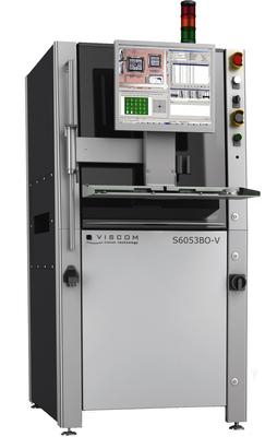
The TR7700QE-S is built on a high precision platform with 5.5 µm high resolution 12 MP imaging technology for the Semiconductor & Packaging industry. The Stop-and-Go 3D AOI is able to inspect wire bonds, die bonds, SMD, bumps, and solder joints. The
Used SMT Equipment | Semiconductor & Solar
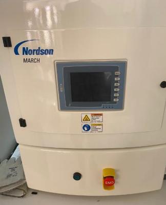
Nordson MARCH AP-300 Plasma System Cleaner 100-230VAC, 50/60Hz, 3.5A @208V, Single Phase A compact and benchtop model, the Nordson March plasma system AP-300 has a volume capacity of 33.1 liters, supported by up to seven (7) adjustable shelves in
Utilise Gold contains an international business directory of suppliers of precious metal materials used in the electronics industry, including contacts, plating salts, pastes, solders, bonding wires and evaporation materials.
Used SMT Equipment | Semiconductor & Solar
Standard Machine features and system description: Ultra-fine pitch and small ball bonding capabilities High frequency transducer operating at 138 kHz Applicable wire size of 0.6mil-2.0mil High speed XY table with linear motor technology High ac
Ma-tek is aimed to be the first tier service lab in the professional field of materials and failure analysis service. Applying a variety of analytical techniques, ma-tek is able to engage the best R&D partnership with customers in high tech industry.
Career Center | , British Columbia Canada | Engineering
Looking for an engineer or technician to do some contract work on the assembly, testing, and failure of analysis of microelectronics packagages. The individual needs to understand the process of gold wire bonding and eutectic die attachment. Knowle

The Bondjet BJ931 High Speed Fully Automatic Dual-Head Wedge Bonder meets the latest technology and flexibility demands for automotive and power electronics applications, handling thin and heavy aluminum, copper and gold wire and ribbon on two specia

.gif)


