Microelectronics Packaging
- STI Patented IC/DT
- Class 1,000 Cleanroom
- Flip Chip & Wire Bond


The Microelectronics Packaging Lab was established to meet the rising need for advanced systems development and packaging to address the emerging challenges and issues facing today’s electronics assemblies. Advanced design and modeling software enables STI to design and develop highly integrated hardware to meet shrinking form and fit factor requirements as well as increasing thermal loads. Emerging packaging materials are continuously evaluated to optimize electrical and thermal performance.
The microelectronics lab specializes in state-of-the-art packaging design and microelectronics assembly including current technologies such as Chip-On-Board (COB) and Multichip Module (MCM) as well as emerging technologies such as STI’s patented packaging technology termed Imbedded Component/Die Technology (IC/DT®).
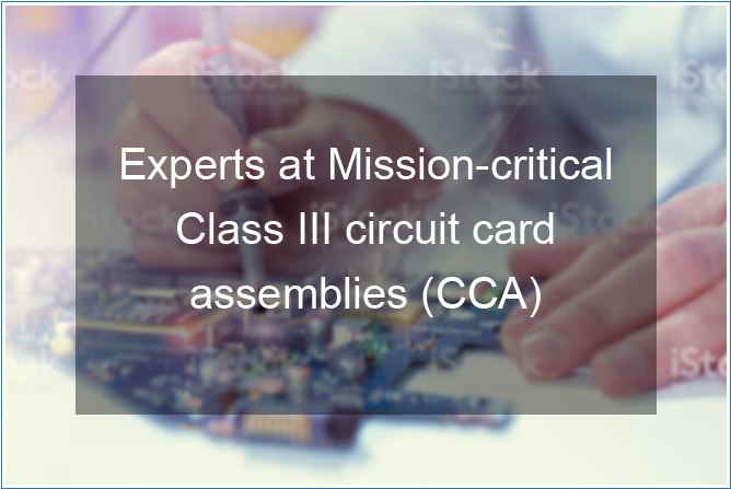
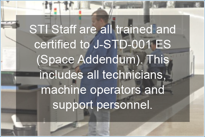
STI’s involvement in research and development programs, both in component packaging technologies and electronics assembly manufacturing, has brought about the installation of the latest and most advanced equipment and the acquisition of the top people in this field. STI is staffed to design, develop, assemble, and test a ruggedized electronics assembly in an advanced cleanroom laboratory (Class 1000/ISO Class 6 certified) to meet our customer’s specifications.
A Class 1000 / ISO Class 6 cleanroom provides the optimum environment for prototype and low volume microelectronics manufacturing and assembly production.
Assembly materials such as printed circuit boards (PCBs), components, and wire are stored in dry nitrogen cabinets to reduce contamination and degradation.
A sophisticated dispenser/placement machine is used for low volume dispense accuracy and repeatability in addition to ±10 μm component placement. Component pick options include waffle pack and wafer for high-precision SMT and bare die, including flip chip assembly.
Wire bond interconnect is accomplished with a fully automatic ultrasonic wedge bonder utilizing aluminum wire over a wide diameter range for low and high current applications.
A two-channel mass flow controller plasma system is employed to prepare surfaces for die attach, wire bonding, and encapsulation.
Material qualification and process control are accomplished via a bond tester coupled with high magnification visual inspection.