A New Light-Weight Electronic Packaging Technology Based On Spray-Formed Silicon-Aluminium by David M. Jacobson
Materials Consultant,
Wembley HA9 8LP
david@jacobson.freeserve.co.uk
Abstract
A new family of silicon-aluminium (Si-Al) alloys has been developed for electronic applications. These alloys are produced using the Osprey spray deposition process which achieves homogeneous and isotropic properties. Their advantageous physical characteristics, combining low thermal expansivity, high thermal conductivity, and low density make them particularly attractive for packaging of avionics, including RF and microwave circuitry. These alloys are easy to machine to tight tolerances using standard machine tools and they can be electroplated with gold, silver or nickel finishes without difficulty. Being non-toxic, they do not require any special handling.
Microwave amplifier modules designed for space applications have been successfully produced and tested. The packages have gold-plated Si-Al bases and kovar side-walls, supplied with appropriate r.f. and d.c. feedthroughs. The lids are laser-welded by conventional seam sealing. This package configuration provides rigid bases for the circuitry and a weight saving of typically 30% over all-kover packages.
Introduction
RF and microwave applications make several difficult demands from packaging materials. Active gallium arsenide devices require a hermetically sealed environment, either locally or package-wide. A metallic enclosure is generally preferred to a ceramic one because it provides superior RF screening. Lead-throughs into the package must be configured to minimise dielectric losses. The packaged circuitry must also achieve good impedance matching.
Efficient heat removal often represents another critical aspect of electronics packaging. In particular, semiconductor devices need to be kept sufficiently cool because failure rates increase dramatically as the temperature of the semiconductor junctions rise. For every 10�C increase in temperature, the lifetime of gallium arsenide (and silicon) devices drops as much as threefold. To promote good thermal management, heat-sinks made of materials with high thermal conductivity or "cold plates" are frequently incorporated into packaging to conduct away heat dissipated by devices. Effective heat sinking is also required to enable circuitry to be packed more densely with components, and thereby made smaller. Another limiting factor in electronics packaging is thermal mismatch stress within the package. Such stresses can cause mechanical failure of devices solder joints, or of ceramic components, when these undergo thermal excursions typical of aerospace environments, that can range from about -50�C to over 100�C.
In short, the ideal material for microwave packaging for aerospace electronics will be metallic, have a CTE matched to, or slightly larger than, those of gallium arsenide and alumina (i.e. about 7 - 9ppm/K), a high thermal conductivity (>100W/m.K) and low density (<3g/cm3). In addition, it is desirable that the packaging material has a reasonable stiffness (> 100 GPa) to provide adequate mechanical support to mechanically sensitive components and substrates. It should also be easily machinable and capable of being plated by an economical and industry-standard method, such as electroplating. Moreover, the ability to seam seal packages of the requisite material by laser welding or otherwise lid them is another important requirement.
A representative range of available materials that are being used in electronics packaging, both for high and low frequency applications, is given in Table 1, together with key property data, namely coefficient of thermal expansion (CTE), thermal conductivity (k) and density (r
).
|
Material |
CTE (at 20�C)
x 10-6/K |
k
Watts/m.K |
r
g/cm3 |
|
Aluminium |
23.6 |
230 |
2.7 |
|
Copper
|
17.6 |
391 |
8.9 |
|
Copper-75% tungsten |
8.8 |
190 |
14.6 |
|
Beryllium-30% beryllia |
8.7 |
210 |
2.1 |
|
Beryllium-51% beryllia |
7.5 |
220 |
2.3 |
|
Beryllia |
7.2 |
260 |
2.9 |
|
Copper-85%tungsten |
7.2 |
180 |
16.1 |
|
Al-68SiC |
6.9 |
150 |
3.0 |
|
Copper-85% molybdenum |
6.7 |
160 |
10 |
|
Alumina |
6.7 |
20 |
3.9 |
|
Kovar |
5.8 |
17 |
8.2 |
|
Titanium |
5.6 |
15 |
4.5 |
|
Molybdenum |
5.1 |
140 |
10.2 |
|
Aluminium nitride |
4.5 |
180 |
3.3 |
|
Silicon-50% aluminium (CE11)* |
11.0 |
140 |
2.5 |
|
Silicon-30% aluminium (CE7)* |
6.8 |
120 |
2.4 |
* as developed by Osprey Metals Ltd.
Table 1: Key property data for materials used for electronics packaging. Values shown in bold are compatible with the requirements for microwave circuitry.
Kovar alloy (54%iron-29%nickel-17%cobalt; note that all compositions given are in weight percent) has been used as the conventional packaging material on account of its coefficient of thermal expansion (CTE = 5.8ppm/K) which is fairly closely matched to those of gallium arsenide (GaAs) and alumina (Al2O3), although on the wrong side. Further on the debit side, this material suffers from a low thermal conductivity (17 W/m.K), high density (8.2 ppm/K), and inadequate specific stiffness (17GPa.cm3/g). In flight systems, there is a severe cost premium attached to weight, with each kilogram of payload made airborne incurring �50,000 over the life of the aircraft, while for satellites, the cost penalties are approximately a hundred times higher than this []: It estimated that a phased-array radar system in an advanced fighter aircraft could be reduced in weight by many kilograms if kovar with a density of over 8g/cm3 were to be replaced by an material having a density of less than 3g/cm3.
There are few materials that satisfy the requisite combination of low density, high thermal and electrical conductivity, suitable CTE and adequate stiffness for RF and microwave packaging [,]. Of these the beryllium-beryllia materials are classified as toxic and their CTE rises faster than that of alumina with temperature, which can introduce significant mismatch stress following brazing and soldering operations.
Other materials that have been developed and are being exploited in this field of application are aluminium-based MMCs [3,,,]. These comprise a matrix of aluminium reinforced with silicon carbide (SiC) particles. This family of materials is difficult to machine and cannot be reliably plated once machined [,]. These materials are difficult to machine owing to the extreme hardness of the contained carbides. However, in recent years pressure casting and pressureless infiltration techniques have been developed for producing net shaped components []. This is achievable up to approximately 68 vol.% SiC content which results in a CTE of ~6.9 ppm /K. The need for hard precision dies means that this route for producing packages is usually only cost effective for large runs (thousands) of identical components. These materials can only be reliably plated, if produced with a continuous skin of aluminium metal. Therefore, a clear need for a new packaging material was identified, particularly one that is expansion matched to GaAs.
The Development of New Family of Packaging Materials
High silicon Si-Al alloys were identified as an attractive materials system on which to base a new packaging technology. These alloys, being rich in silicon, all have a low density (<2.5 g/cm3 ) and contain cheap and widely available constituents, aluminium and silicon in the form of electronic scrap. They are also environmentally friendly, being perfectly safe from a health point of view and not posing any disposal problems.
A project sponsored by the European Union under its BRITE/EURAM R&D programme (Project BE5095-93) was undertaken to develop Si-Al alloys rich in silicon, assess their properties and to evaluate their suitability for use in light-weight, low CTE packaging. This involved a close collaboration between the materials supplier, Osprey Metals Ltd., and two end-users, Alcatel Space and GEC-Marconi Ltd., which helped to tailor the new materials to end-user requirements. The project achieved its objectives and this has led to the new CE (controlled expansion) materials being launched on the market [,].
As their name indicates, these controlled expansion alloys have the advantage of having any desired CTE value between those of aluminium (23.6ppm/K) and silicon (2.2ppm/K), simply by varying the relative proportions of silicon and aluminium. Fig. 1 shows the variation of CTE at 20�C with silicon content in the alloy.

Figure 1 : Coefficient of thermal expansion (CTE) of spray-deposited Si-Al alloys as a function of silicon content.
The CE alloys possess other desirable characteristics for packaging applications. They are up to 15% lighter than pure aluminium and more so than the high strength aluminium engineering alloys. Their CTEs do not vary greatly with temperature, changing by no more than 10% from -50�C and 300�C, making them compatible with alumina and GaAs in this repect. Their elastic modulus exceeds 110 GPa, and taken in conjunction with their low density, they possess very high specific stiffnesses (53 GPa.cm3/g in the case of the Si-30Al (CE7) alloy, as compared with only 17 GPa. cm3/g for kovar and 15 GPa.cc/g for Cu-75W).
Historically, the use of high silicon Si-Al alloys has been hampered by their mechanical fragility associated with the presence of large columnar grains of silicon, when the alloys are produced by conventional chill-casting. It was anticipated that this limitation might be mitigated by preparing them using a process that results in a fine and isotropic microstructure. Such a process, which is capable of output on an industrial scale is one employing spray deposition, as developed by Osprey Metals Ltd [,].

Figure 2: Micrograph showing the uniform, isotropic microstructure of the spray-cast Si-30 wt% Al (CE7) alloy.
In the Osprey process, a stream of the chosen metal or alloy is inductively melted. The molten metal is directed through a nozzle and atomised by nitrogen at high velocity, creating small droplets which are typically ~40�m in diameter. These droplets condense onto a cold, rotating plate. The coalescing droplets undergo rapid cooling resulting in a relatively fine isotropic microstructure. At this stage, the boules contain some porosity which is reduced to less than 1% by hot isostatic pressing. A micrograph showing the uniform, isotropic microstructure of the densified alloy, of composition Si-30%Al, is shown in Fig. 2.
The thermal conductivity of the densified Si-30%Al alloy is 120W/m.K, while its electrical resistivity is less than 10-6 W
.m at 20�C, while its CTE is 6.8ppm/K at the same temperature (see Table 1).
Fabrication of Electronic Packages of CE Alloys
Prototype microwave integrated circuit (MIC) packages have been fabricated by machining using either milling with tungsten carbide tools, and then plated with nickel and gold. typical packages weigh about 6g, which compares with ~20g for a corresponding kovar package.
Two types of microwave package configuration are being investigated. One of these is the �heterogeneous� type, in which kovar side-walls with glassed-in feedthroughs are hermetically attached to machined baseplates of the CE alloy. A second, more ambitious, type of package is �homogeneous,� i.e. entirely constructed of the CE alloy. In this latter type, the package and sidewall are fashioned from a single piece of the material and planar feedthroughs are attached to the sidewall. The �heterogeneous� approach has been used for packages that are being developed for solid state power amplifiers (SSPAs) for space applications. The manufacture of these packaging involves:
- 1. Machining baseplates and carriers of the CE alloy to the requisite geometries and surface finishes, using tungsten carbide tools.
- 2. Plating the baseplates and carriers to provide a gold finish to achieve stable r.f. ground-plane for microwave circuitry.
- 3. Hermetic attachment of kovar sidewalls with glassed-in feedthroughs onto gold-finished baseplates of CE alloy.
These features of these process steps will be described in further detail.
Machining
It has been demonstrated that machining of these high silicon alloys can be routinely accomplished using titanium nitride (TiN) coated carbide tooling, to an average surface roughness (Ra) of better than 1.6 �m, provided that the silicon content in the CE alloy is less than 80%. When optimised, the machining also produces crisp edges. It is also possible without much difficulty to avoid causing break-out at the edge of drilled holes. The finest detail can be achieved using tools coated with a thin layer (~10�m), of polycrystalline diamond (PCD). A representative housing for a channel amplifier, comprising a mixed L.F./R.F. multichip module, to an Alcatel Telecom design is shown in Fig. 3 []. This housing was composed of a spray-cast Si-50%Al alloy that was PCD machined at Alcatel-Telecom and gold plated at GEC-Marconi Materials Technology Ltd.
Non-circular slots and recesses can be readily produced in the CE alloys by electro-discharge machining (EDM). These materials can also be laser cut with ease. This technique is most suitable for producing thin slices and fine detail.
Plating
The CE alloys are routinely electroplated with commonly employed silver or gold finishes, using procedures based on those used for aluminium and its alloys [1,2]. These involve establishing an electroless nickel layer on the surface and then carrying out a sequence of operations leading up to a final finish of gold or silver to the required thickness.
The coating process has been optimised so that the metallisation survives a blister test involving a 450�C bake followed by an ultrasonic exposure at >104 W/m3 and a hot humidity exposure (65�C, 95% relative humidity, for 72 hours). Plated components tested under shear or bending loads have consistently failed in the bulk of the material rather than at the interface with the coating.
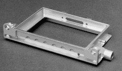
Figure 3: A channel amplifier housing, about 80 x 50 mm x 10 mm to an Alcatel Telecom design, machined from Si-30 %Al (CE7) alloy using polycrystalline diamond (PCD) tools at Alcatel Telecom and gold plated by GEC-Marconi Materials Technology Ltd.
Joining Sidewalls to Baseplates
Kovar sidewalls are attached to gold plated CE baseplates using high temperature Au-Sn or Au-Ge solders, by methods that are now fairly standard. Diffusion soldering has also been used with success. This process involves melting a solder in the joint, which then reacts with and diffuses into the metallisation on both sides of the joint, such that the joint solidifies isothermally to provide a higher remelt temperature than the joining temperature []. Diffusion soldering enables the joining operation to be carried out at a temperature below 400�C but the joint that forms will withstand much higher temperatures without melting and they have the additional benefit over conventional soldering of being virtually void-free when the process is operated under optimum conditions.
Package Manufacture
Device carriers and packages have been designed, manufactured and populated with electronics circuitry. One of the completed packages has a base plate of the CE7 alloy, with a recess machined in to receive a 10W r.f. 1Ghz amplifier device, shown in Fig. 4. In this example, the amplifier delivered 8W of power. The substitution of the kovar base with one of CE7 results in a weight saving of 30% without, in any way, compromising the performance of the amplifier.

Figure 4: A populated 10 W power amplifier (1GHz) package with a CE7 base. The package measures approximately 50 mm square.
Conclusions
The requirements for microwave packaging materials have been reviewed and the essential properties that considered important for aerospace applications have been highlighted. A new series of silicon-aluminium (CE) alloys have been developed which address these critical requirements. They are environmentally friendly and have excellent manufacturability, being straightforward to machine and electroplate. In turn, these characteristics make their use in package prototyping and small production runs highly cost competitive.
Apart from RF and microwave housings and carriers, other parts of high frequency systems will benefit from the new CE materials from Osprey Metals. These include waveguide and microwave filter components, which can use to advantage the good thermal stability, stiffness and platablility of these materials.
Further work has been initiated to develop packages of all-Si-Al alloy construction (�homogeneous� packages). Trials to hermetically solder stripline feedthroughs with microstrip connections into the CE alloy side-walls, plated with gold, and laser weld CE alloy lids onto these packages have been successful. It is planned to continue this development work.
Acknowledgements
Acknowledgements are due to Dr Andrew Ogilvy of Osprey Metals Ltd and to Dr Satti P.S. Sangha of Matra- Marconi Space UK Ltd for their contributions in developing the silicon-aluminium alloys and the packaging technology. Michel Azema of Alcatel Telecom is acknowledged for the machined channel amplifier housing shown in Fig. 4.
REFERENCES
[1] D. White, S. Keck, I. Smith and A. Silzars, "New ground in hybrid packaging," 1990, Hybrid Circuit Technology, 12 ( 1), 14-19.
[2] D.M. Jacobson and S.P.S. Sangha, "Future trends in materials for lightweight microwave packaging, 1998, Microelectron. Intl., 15 (3), 17-21.
[3] C. Zweben, "Advances in composite materials for thermal management," 1998, JOM 50 (6), 47-51.
[4] K.A. Schmidt, B.T. Rodini and C. Zweben, "Composite packaging materials", in Electronic Materials Handbook, Vol. 1, Packaging, 1989, Materials Park, Ohio, ASM International, 1122-25.
[5] K.A. Schmidt and C. Zweben, "Application of composites in packages," 1989, ditto, 1126-28.
[6] B.E. Novick and R.W. Adams, "Aluminium / silicon carbide (AlSiC) metal matrix composites for advanced packaging applications," 1995, Proc. 1995 Intl. Electron. Packaging Conf., IEPS, San Diego, CA, Sept. 24-27 1995, 220-27.
[7] R.F. Jeffries and D.J. Burrows, "Metal Matrix Composite Packaging of Microwave Circuitry", 1994, GEC J. Res., 11 (3), 150-66.
[8] A.R. Chambers, "The Machinability of Light Alloy MMCs," 1996, Composites A, 27A (2), 143-47.
[9] D.J. Lloyd, "Particle Reinforced Aluminium and Magnesium Matrix Composites", 1994, Intl. Mat. Rev., 39 (1), 1-23.
[10] S.P.S. Sangha, D.M. Jacobson, A.J.W. Ogilvy, M Azema, A Arun Junai and E Botter, "Novel Aluminium Silicon Alloys for Electronics Packaging", 1997, Eng. Sci. and Educ. J., 6, 195-201.
[11] D.M. Jacobson and S.P.S. Sangha, "A novel lightweight microwave packaging technology," 1998, CPMT(A), 21 (3), 515-20.
[12] A. Leatham, A. Ogilvy, P. Chesney and J.V. Wood, "Osprey Process - Production. Flexibility in Materials Manufacture", 1989, Metals & Materials, 3 (3), 140-43.
[13] A. Leatham, "Spray Forming Technology", 1996, Adv. Mats. & Procs., August, 31-34.
[14] C. Drevon, S. George, A. Coello-Vera, M. Pouysegur and J.L. Cazaux, "Mixed L.F./R.F. MCM", 1997, Proc. 47th Electronic Component and Technology Conference, San Jose, California, 18-21 May, 1997, New York, IEEE, , 497-501.
[15] D.M. Jacobson and S.P.S. Sangha, "Novel Applications of Diffusion Soldering,' Soldering & Surface Mount Technology, Vol. 23, No. 1, 12-15, 1996.
|