NO HASL - WHAT'S THE HASSLE?
The type of PCB finishes can directly affect results and performance at In-circuit Test. With the pursuit of lead free PCB finishes, the test development engineer now has something new to worry about.
The type of PCB finishes can directly affect results and performance at In-circuit Test. With the pursuit of lead free PCB finishes, the test development engineer now has something new to worry about.
Jon O'Connell, Agilent Technologies UK Limited
BACKGROUND
Historically, the test engineer has been primarily concerned with ensuring he has an effective test program that performs well in production. In -Circuit test is still a very effective method of detecting manufacturing defects. More advanced ATE systems can also add real value at test in providing means to program flash memory, PLD's, FPGA and EEPROM. Agilent's 3070 ICT system is at the forefront of this field It's established that In-Circuit test(ICT) still has plenty to offer to the manufacture and testing of PCA's, but how will the pursuit of a lead free PCB affect the ICT stage?
The push for lead free solder techniques has lead to many investigations into PCB finishes. These have been primarily based on the technology performance during the build process. The effects that the PCB finish has at test phase has mostly been overlooked or focussed on contact resistance. This report will present details of the effects seen at ICT and the need to respond and understand these changes. The purpose of this document is to share in these experiences and educate engineers as to where different PCB surface finishes require a different fixture approach. This is the first paper to address lead free PCB finishes issues specifically at In circuit test stage of manufacture. The test engineer needs to ensure that he is included in trials for lead free PCB. The RoHS directive comes into place for the EU in 2006.
WHAT'S THE HASL ANYWAY?
Before we look at cause and effect, it's important we should know about the types of PCB surface finishes available and what they offer.
All Printed Circuit Boards(PCB's) have copper finishes on their surface. If they are left unprotected then the copper will oxidise and deteriorate, there are various protective finishes available, namely:
- Hot air solder levelling (HASL)
- Organic Solder Preservative (OSP)
- Electroless-Nickel Immersion Gold (ENIG)
- Immersion Silver and Immersion Tin
HASL is the predominant surface finish used in the industry. The process consists of immersing circuit boards in a tin/lead alloy and the excess solder is then removed by 'air knives', which blow hot air across the surface of the board. For the circuit board manufacturer, the HASL process is expensive and maintenance intensive. Not to mention the increased health and safety hazards. For the printed circuit assembly (PCA) process, HASL has many advantages. It is the cheapest PCB available and the surface finish remains solder able through multiple reflow, wash and storage cycles.
HASL has been working well for many years but with the advent of 'greener', more environmentally friendly processes, it's days are numbered. In addition to the lead free movement, the increased complexity of boards and finer pitches has exposed many limitations with the HASL finish.
Pro's: Lowest cost PCB's, remains solderable through whole manufacturing process, no negative effect at ICT
Con's: Uses lead process which is currently restricted and eventually eliminated by 2007, for fine lead pitches (<0.64mm) can lead to solder bridging and thickness issues, unevenness of finish causes co planarity problems in assembly process.
What does it look like? PCA's test points and via holes will have solder covering.
Organic Solder Preservative (OSP)
OSP is designed to produce a thin, uniform, protective layer on the copper surface of the PCB's. This coating protects the circuitry from oxidisation during storage and assembly operations. It has been around for quite a while but is only recently gaining popularity with the search for lead free techniques and fine pitch solutions. For PCB manufacturers it's very simple and easy to control. For PCA assembly, it has superior capabilities over traditional HASL with regard to coplanarity, solderability but requires significant process changes with the type of flux and number of heat cycles. Careful handling is needed as acidic fingerprints degrade the OSP and leave the copper susceptible to oxidisation. Assemblers prefer to work with metal finishes that are more flexible and endure more heat cycles. It also causes major problems at ICT with the bed of nails fixture contact. More aggressive probing is required to break through the OSP layer which could potentially even lead to damage and piercing of the PCA test via's or testpoints.
Pro's: Comparable per unit cost to HASL, excellent coplanarity, lead free process, improved solderability, no 'black pad' issues.
Con's: Significant changes needed to assembly process, not ICT friendly, aggressive ICT fixture probes can potentially damage the PCB, manual handling precautions needed, ICT limits and repeatability compromised.
What does it look like? There will be no solder on testpoints, operators handle OSP boards with gloves, OSP thickness and presence is difficult to ascertain.
Electroless-Nickel Immersion Gold (ENIG)
These coatings have been used with great success on many boards despite the high per unit cost. It has a flat surface and excellent solderability. The main drawback is that the electroless nickel layer is brittle and has been found to break up during mechanical stress. This effect is known in the industry as 'black pad' or 'mudflat cracking'. This has lead to bad press for ENIG, if these problems could be overcome this finish would be the ideal coating - apart from the incremental cost.
Pro's: Excellent solderability, coplanar - flat surface, excellent shelf life, withstands multiple reflows
Con's: Higher cost (approx 5x HASL), 'black pad' issue, manufacture process uses cyanide and other unpleasant chemicals.
What does it look like? Gold plated finish on pcb joints
Immersion Silver
Immersion silver is a relatively recent addition to the PCB finish. It's main use has been in Asia and is gaining popularity in North America. Europe now has emerging market. During the soldering process the silver layer gets dissolved into the solder joint leaving a tin/lead/silver alloy on the copper which provides very reliable solder joints for BGA packages. The contrasting colour makes it easy to inspect, as opposed to OSP. It's also a drop in replacement for HASL for soldering operations. There is although an underlying question mark over silver 'migration', but newer finishes have anti-migration agents added to minimise the effect. Immersion Silver is a very promising finish but end users are very conservative. Many customers place this finish as 'under investigation', but it may well emerge as the best finish. There have been some initial studies into reliability at ICT and it has emerged that etch time (surface rough/shiny) and thickness of finish are important considerations regarding repeatability. There are no suggestions that there will be any negative effects seen at in circuit test stage.
Pro's: Good solderability, coplanar - flat surface, 'drop in' replacement for HASL
Con's: Slow uptake of technology.
What does it look like? Silver finish appears 'white' on PCB surface.
Immersion Tin
Immersion tin is a newer alternative surface finish, with many similar characteristics to it's silver counterpart. However, there are major health and safety issues to consider. It is mainly used in Europe and Asia whilst it's use in the US is restricted due to the concern over the thiourea used in tin solution (a suspected carcinogen).
Pro's: Good solderability, flat surface, relatively low cost
Con's: Heath and Safety concerns, limited number of heat cycles
What does it look like? Tin finish appears 'white' on PCB surface.
SUMMARY
PCB Surface Finish Summary
These are the main players in the PCB finish arena. HASL continues to be the most widely used PCB finish and in this case the test engineer will not see any differences. In some countries, HASL is already outlawed and alternatives are in place. With PCA manufacturing spread across a more diverse and global arena the possibilities of seeing non-HASL finishes at In-Circuit test are increasing. OSP is not the natural replacement for HASL but in despite of that it has been one of the first alternate finishes that PCA manufacturers try out which is leading to real test reliability issues at ICT.
The conclusion is that there is no 'holy grail' of PCB finishes, each have there own set of issues that need consideration and some are worse than others. The facts are that these different PCB finishes will need adaptation at the ICT stage.
PERFOMANCE AT IN CIRCUIT TEST (ICT)
HASL vs. OSP vs. Silver
I want to now turn the focus to these technologies and how they could impact performance at ICT.
HASL
HASL finishes leaves soft solder 'domes' on testpoints and unmasked vias that are perfect target for ICT probes. What HASL does and OSP cannot is to absorb force. HASL is eutectic SnPB, which is extremely soft. This soft target does two things, it adapts to the probe and it absorbs energy.
OSL
Copper is a pretty hard surface in comparison and cannot absorb much energy therefore the immediate contact area for the probe to bite into is reduced. The copper plating on the outer layer is typically between 10 - 50um. Combine that with the OSP covering layer, you can see that the probe that you used to probe the HASL boards is not going to perform on the OSP finish boards. Studies show that the longer the time between reflow and ICT, the OSP can create a hard 'crust' on test targets. Optimum transfer time to ICT is <24 hours. There are very many other process factors that can influence how much OSP will be a problem for the test engineer, such as, OSP vendor type, number of times through reflow oven, has wave process been removed, nitrogen vs. air reflow, and what amount of low value analog measurements are you making at ICT.
OSP effects at ICT have been such a problem for some PCA manufacturers they have totally outlawed it's use. Others have learnt to live with it and worked to a set of 'OSP rules', which involve changing probe styles to high force and sharper angle, repeated vacuum 'hits' and opening test limits. OSP is deemed by some to offer immediate cost savings and to be the first choice replacement, however, some companies have recently made a u-turn and are re-examining their strategy when the real costs associated in manufacture delays are accounted for.
Problems occur because we are probing directly onto the copper surface which has a far reduced thickness compared to HASL or other finishes. Combine a PCB like this with the higher probe force needed to break through the OSP layer and perhaps using micro via's as testlands , then you have a real potential to break through that thin copper layer and go through to the layers underneath, In turn causing internal shorts.
In recent cases it has been seen that a board via or testpoint has been pierced in anything between 5-10 actuations of the fixture ! - which may work well enough for production purposes, but if a board has to go through a significant number of repair cycles or is used for debug & verification, then it's a different story.
Immersion Silver
Immersion Silver thickness is typically 0.4 to 0.8 um on top of the copper layer so offering some 'meat' for the test probe to bite into. Silver is not as widely used as HASL or OSP, but initial studies have shown it to be a 'drop in' replacement for HASL as far as the manufacturing process. As for it's performance at ICT there have been studies as to how the thickness and etch time can affect performance.
The etch rate is important to ICT testing as it determines whether the silver finish will be shiny or matt. A direct result of the etch rate is not only to provide secondary cleaning of the copper surface, but to also micro-roughen the surface which increases the surface area. During the silver deposition step, the silver takes to the contours of the copper surface. Therefore, the surface with increased roughness, hence area, presents a matt finish - the surface with minimal roughness presents a shiny finish.
There should be no need to adapt ICT probe forces or styles to test these boards. There have been very limited studies of this finish but technically and commercially it would seem that this is the most promising. PCB manufacturers are now offering silver finish boards at the same cost as their HASL counterparts.
PCB summary table
| Assy Technology | PCB Finish | |||
| HASL | OSP | Silver | Gold | |
| Fine Pitch | > 0.5mm | <<0.5mm | <<0.5mm | <<0.5mm |
| Coplanarity | Poor | Excellent | Excellent | Excellent |
| Wave Soldering | Excellent | Good | Good | Good |
| Reflow Soldering | Excellent | Good | Good | Good |
| Press Fits | Good | Good | Excellent | Good |
| ICT Probing | Good | Poor | Good | Good |
Customer Trial Results
I can share some data that was initiated by a customer when they saw significant impact to yields when introducing OSP PCB finish as a lead free replacement on one of their product lines. These are independent results captured by the customer and are not influenced by Agilent in any way. The test equipment used was the market leader Agilent 3070 in circuit tester which is widely accepted as being the most stable test platform in industry. The specifications for the trial are as follows:
*Agilent Comment
These results are direct from customer survey and are not reflective of Agilent Technologies, Inc. opinion and are only looking at HASL and OSP fnishes.
| Area | Parameter | Fixed or Variable | Comment |
| Test Dept | Probe force | Varied 2N- 3N | 2N sufficient for HASL |
| Probe style | Varied | Daggers, Triads | |
| Probe Mfr | Fixed | Ingun | |
| Probe Maintenance | Fixed | Optimised | |
| Probe Age | Fixed | New Probes | |
| Probe Pitch | Fixed | Optimised | |
| Test Software | Fixed | Agilent 3070 ICT | |
| Batch Size | 50 boards | ||
| Process | Post reflow delay | Variable | <24 hours |
| Handling | Fixed | Gloves used |
Customer Survey Results and Observations
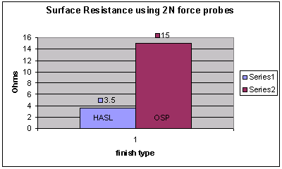
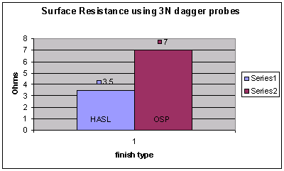
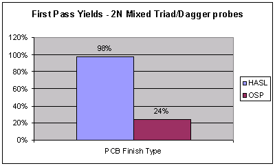
Observations
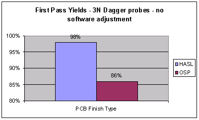
- Dagger probes perform significantly better than the triad probe.
- Higher force probes are required in the fixture to counter affect of OSP - from 2N to 3N
- Even with changes to probe style and force there need to be relaxation of test limits for shorts test and small value analog in circuit tests in order to achieve a reasonable first pass yield. This effort can be siginificant dependant on board type.
- Financial impact of additional resource and fixture re-probe should be accounted for when looking at unit cost saving for OSP finish PCB.
- Insufficient evidence was available to determine what effect pure nitrogen reflow process would have. More exhaustive studies were required. Although it is considered that the processes were as near perfect for OSP as could be achieved.
Summary
It seems that the trend has been for OSP to be seen as a natural replacement for HASL. This decision is most probably derived from perceived unit cost savings. Indications show that this should be a concern as OSP and ICT do not perform well together. The performance and effort required to adapt processes to attain anything like a first pass yield increases dramatically. What would seem to be an initial cost saving opportunity can be negated by the costs of changing fixture probes, maintenance, adapting test software and scrap costs of damaged boards.
We have seen many recent u-turns on OSP decisions in favour of Silver. The general feeling is that customers don't like OSP, however, it does provide a low cost lead free PCB solution. The advice for those customers who have not changed from HASL yet is to make sure that you are fully aware of the pro's and con's of all viable lead free PCB alternatives and to ensure that all manufacturing stages are included in trials - Including Test!
Unfortunately we do not have any definitive data available for Silver PCB finishes with respect to ICT and any inputs would be welcome.
Sources and Acknowledgements
Evaluation of Immersion Silver Finishes for automotive electronics: Robest Gordon, Susan Marr, Dongkai Shangguan - Visteon Corporation
The Quest for the Ultimate Surface Finish: Luc Beauvillier - Printed Circuit Design June 2002 edition
Thanks to:
Helmut Kroener - Multek Europe
Paul Owens - 3Com Ireland
Steve Changelon (US), Steve Doherty (UK), John Kirby(UK), Jun Balangue (Singapore) - Agilent Technologies, Inc.