Nov 05, 2019
PCB Panelization
To achieve some economy of scale, several PCB designs can be placed or repeated on a large PCB panel. Panel size varies by manufacturer, but the real limit on panel size is what the automated assembly and test machines the PCB assembly house can use. Using a PCB panel with many copies of a PCB board on it reduces the cost for automated assembly by limiting the setup time for each PCB.
The panelization of a PCB design needs to include several features and marks to support the automatic assembly process as well as removal of the individual PCB boards.
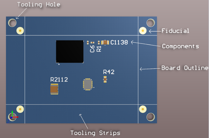
Tooling Strips - The machines that assemble and test PCB boards require some space to hold the panel as it moves through the machine. These areas are called the tooling strips and are on the top and bottom edges of the panel. They also contain tooling holes, manufacturing information, and location marks that are required to guide the panel through the assembly process. At least four tooling holes are required per panel, with hole sizes being specified by the assembler.
Fiducial Marks - Fiducial marks are used to provide visual alignment points for the automatic assembly of a PCB. They serve as reference points for the optically aligned pick-and-place CNC machine that picks up and places all of the surface mount components on the PCB board. Each Panel needs at least 3 fiducial marks to provide alignment for all of the parts on the panel. These marks are known as the global fiducial marks and are typically placed on the tooling strip as 1.5mm diameter copper pads that are at least 5mm away from the edge of the panel. Local fiducial marks are also required around all large, fine pitched surface mount chip to provide at least two local points of reference to ensure good alignment between the part and the pads
Soldering - How the PCB will be soldered has an impact on the design of a PCB panel. There are three primary types of soldering techniques used today, wave soldering, reflow soldering, and hand soldering.
Hand soldering is the traditional manual method of soldering which is good for prototypes and small production runs where manual labor costs are lower than setup costs for automated soldering methods. If hand soldering will be used, the layout of the PCB must ensure that there is enough clearance between parts to maneuver a soldering iron and that each pad has enough area for a thermal relief.

Wave soldering is a soldering technique where the PCB board is passed over a bath of molten solder. The process works well for both surface mount and through hole components. Since the entire board is covered with a bath of solder, solder masks to prevent bridging of pads and contacts is essential. The PCB layout also needs to accommodate the 'shadow' of larger components that will prevent the solder from reaching small components directly behind them as they pass through the solder bath. A glue check target is another important PCB panel feature if wave soldering is used as small surface mount components are glued in place before the board is not through the solder bath. A wave break is also needed on the PCB panel, which 'breaks the wave' of the solder bath and keeps the solder bath on one side of the PCB. A wave break should be about 0.5" wide and placed so that it is the first part of the panel entering the solder bath.

Reflow soldering is a soldering technique specifically for surface mount components. Before the PCB panel has components places on it, all of the pads on the board are coated with a solder paste. Once each component is placed and possibly held in place with glue, the entire board is placed in an infrared oven and baked to melt the solder paste. The solder paste melts and reflows on the pads and components to make a solid joint. If glue is used to hold the surface mount components in place, a glue check target will be required on the tooling strips. Reflow soldering is more complex and expensive than wave soldering, but allows the densest placement of surface mount components and avoids the wave solder 'shadow' of large parts.

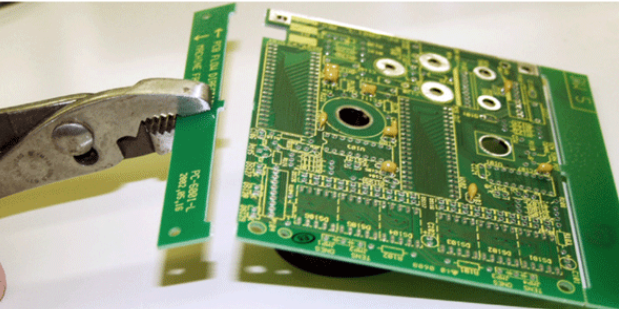
De-panelization - Once assembly is complete, a way to remove each individual PCb board is required. Three of the most common de-panelization methods are routing around the board, using several small 'break-out" tabs around the perimeter, and using a V groove. The break-out tab involves drilling lot of small holes where the PCB should break apart. When the board is ready to be removed, the break-out tab can be cut with a pair of snips to release the board. This method does leave slight nubs on the PCB when the break-out tab is cut. The V groove method uses a score mark around the individual PCB to allow the PCB to be easily snapped along the grove. This results in a smoother edge than using break-out tabs. The best edge is given by fully routing the perimeter of the PCB board. Unfortunately it is also the most expensive and heavy components on the board can cause problems as the board is being routed out.