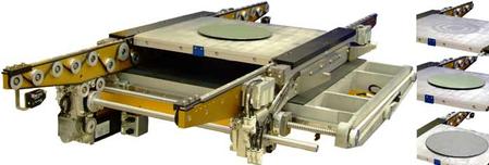
Accommodating modern, thin wafers down to 75um in thickness is achieved through an advanced wafer pallet designed to deliver proper support and stability for delicate wafer dimensions. The DEK precision wafer pallet is flat to less than 10um within the critical process area and can manage wafers as large as 300mm, holding them securely while allowing successful processing for a host of sophisticated packaging techniques. In addition, the newly engineered rail system provides the precise, stable movement control required for transfer of the loaded wafer pallet in and out of the platform, ensuring exceptional control of speed, acceleration and positioning. While the Wafer Transport Solution will be shown on board the Galaxy at Semicon West, the technology is available on several of DEK’s leading platforms including the Horizon 02iX, the Horizon 01iX and the Europa.
David Foggie, DEK Semicon and Alternative Applications Manager, explains the significance of the Wafer Transport Solution: “As processes become more advanced with much thinner wafers, finer pitches, thinner and smaller deposits and exponentially reduced solder sphere dimensions, they put much greater demands on the printer to reliably and precisely deposit controlled amounts of material. DEK’s Wafer Transport Solution contributes directly to this objective of improved process control by maintaining superb flatness and control of the thinned wafer while simultaneously allowing for comparatively high UPH. The versatility of the system enables successful implementation of a number of processes including wafer bumping, ball placement, protective wafer coatings, die attach paste deposition, conductive inks and glass frit or adhesives application for MEMS, among others.”
“It is important to note,” Foggie continues, “that CHAD’s WaferMate wafer handling technology is also a key component of process success.” During the July 13 – July 15 Semicon event, DEK will display the Galaxy solution in-line with CHAD’s WaferMate 300-1 transport system. Encompassing thinned and warped 300mm wafer handling capability, WaferMate delivers the flexibility to move wafers or paper from a coinstack configuration and incorporates advanced technology to limit wafer contact during transfer to the wafer pallet.
Combined, the Galaxy with Wafer Transport Solution and the WaferMate 300-1 deliver a complete in-line system capable of throughput of up to 60 wafers per hour. Add to this Galaxy’s alignment accuracy of 2Cpk@+/- 12.5um, wafer backside coating capability of 2 Cp @+/- 12.5um with a total thickness variation (TTV) of 8um and wafer level ball placement yields in excess of 99.99% for 200um diameter spheres and above, and the total solution is untouchable in terms of accuracy, UPH and efficiency.
“In addition to its outstanding performance, the DEK-CHAD pairing affords users multi-application capability, which likely makes the system one of the most cost-effective market-ready packaging process solutions available,” concludes Foggie. “And, even though the Wafer Transport Solution has been proven on processes which are years from becoming mainstream, DEK continues to push the envelope and is already working on next-generation advances such as 50um wafer imaging, high-yield 100um ball placement and unique vision alignment technologies.”
To find out more about the DEK Wafer Transport Solution and the CHAD WaferMate 300-1, please visit the DEK-CHAD booth, #5251 in the North Hall of San Francisco’s Moscone Center, from July 13 through July 15 2010. Additional information is available online at http://www.dek.com and http://www.chadindustries.net.
DEK is a global provider of advanced materials deposition technologies and support solutions including printing equipment platforms, stencils, precision screens and mass imaging processes used across a wide range of applications in electronics pre-placement subassembly, semiconductor wafer manufacture, and alternative energy component production. For more information, visit DEK at http://www.dek.com


