New Equipment | Education/Training
IPC standards, the results of industry consensus and collaboration, are respected throughout the whole world. Using IPC standards allows manufacturers, customers and suppliers to speak the same language. IPC standards are used by the electronics
New Equipment | Education/Training
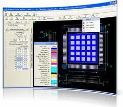
IPC-7351B includes both the standard and an IPC-7351B land pattern calculator on CD-ROM for accessing component and land pattern dimensional data.The calculator includes the document’s mathematical algorithms so users can build a land pattern for a c
Electronics Forum | Fri Mar 29 10:51:20 EST 2002 | lsmith
The IPC-EM-782 reads as follows: the adjustment factor is usually intended to increase the Z dimension slightly, but brings the Z maximum up to an even equivalent. Example if Zmax is 2.100mm then you would enter an adjustment factor of .100mm. The ad
Electronics Forum | Sat Sep 11 13:45:23 EDT 2021 | kojotssss
Hi, check the Land pattern 0201 on the board, compare with another 0201. Could be different gap.,
Industry News | 2010-07-22 22:37:02.0
IPC — Association Connecting Electronics Industries® has released the B revision of IPC-7351, Generic Requirements for Surface Mount Design and Land Pattern Standard. The leading industry standard for surface mount land pattern design and layout, IPC-7351B provides designers and printed board fabricators with updated guidance on requirements of land pattern geometries used for the surface attachment of electronic components, as well as surface mount design recommendations for achieving the best possible solder joints.
Industry News | 2017-05-11 17:06:16.0
Library Expert Lite automatically builds footprints and 3D STEP models for tens of millions of parts, for free.

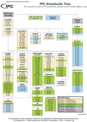
IPC Vice President David Bergman explains where to find and how to use the Document Revision Table.
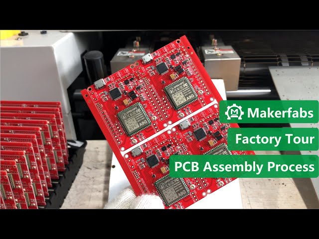
In the world of makers, people enjoy the fun of designing and developing hardware/ software, even final electronic products. They will not concentrate a lot on the cost and manufacturability. But it is quite different from lab to factory, when it com
| https://unisoft-cim.com/crosschecking-pcb-component-footprint-and-bom-footprint.html
(correct solder pad size and land pattern) for the same component listed in the Bill of Materials (BOM). The mismatch of component footprint spacing is usually an error created when components on the PCB assembly ( PCBA
Surface Mount Technology Association (SMTA) | https://www.smta.org/smtai/courses.cfm
. Recommendations will be furnished regarding unique SMT land pattern reinforcement criteria, cover layer and fiducial requirements for automated assembly processing will be defined including detailed


